
Add to Cart
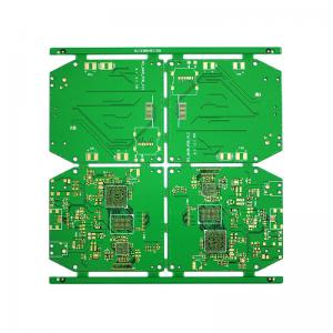
Multilayer PCBs (Printed Circuit Boards) or PWBs (Printed Wiring Boards) are boards that are composed of several layers of electrical circuit materials, like FR4, which are sandwiched together. These boards are widely used in the electronics industry, and are capable of performing multiple functions. With the ability to accommodate up to 64 layers, these Multilayer Printed Circuit Boards and Wiring Boards are extremely versatile and are able to handle a wide range of applications.
The Multilayer Printed Circuit Boards and Wiring Boards are manufactured with advanced technologies to ensure that they have a high quality and reliable performance.
| Parameter | Value |
|---|---|
| Board Size | Customized |
| Board Thickness | 0.2-10mm |
| Layer Count | 2-64 |
| Surface Finish | HASL/ENIG/OSP/Immersion Gold/Immersion Tin/Immersion Silver |
| Silkscreen Color | White/Black/Yellow/Red |
| Copper Thickness | 0.5-12oz |
| Solder Mask Color | Green/Blue/White/Black/Yellow/Red |
| Material | FR4 |
| Min. Hole Size | 0.2mm |
| Min. Line Width/Space | 3/3mil |
Multilayer Printed Circuit Board (PCB) from Cesgate is the perfect solution for electronic devices with complex wiring. The required circuits are made on the front and back surfaces of multiple double-sided boards, and an insulating layer (Prepreg) is sandwiched between the two double-sided boards and then pressed together to form several layers of copper. The construction of the wire is usually an even number of layers due to the use of multiple double-sided laminates. The number of copper wires that can be made by multi-layer boards is the largest, and it is used in more complex circuits. At present, the motherboards used in computers mostly use eight-layer boards because of too many components. Generally, small electronic products, such as mobile phones, tablet computers, etc. Due to the requirement of small size, at least an eight-layer board is required. The more electronic components, the smaller the product size, and usually more layers of PCB are required.
Brand Name: Cesgate
Model Number: NA
Place of Origin: China
Certification: UL,IATF16949,IS09001,ISO14001
Minimum Order Quantity: 1PCS( NO MOQ)
Price: $1.00
Packaging Details: PCB: Vacuum Packing / PCBA: ESD + vacuum Packing
Delivery Time: 3-7 working days
Payment Terms: T/T, L/C
Supply Ability: 13kk soldering spot/day
For Customized Multilayer Printed Wiring Board, Multi-Layer wiring Board, Multilayer Printed Wiring Board:
Layer Count: 2-64
Surface Finish: HASL/ENIG/OSP/Immersion Gold/Immersion Tin/Immersion Silver
Board Size: Customized
Solder Mask Color: Green/ Blue/ White/ Black/ Yellow/ Red
Silkscreen Color: White/Black/Yellow/Red
Multilayer PCB offers a wide range of technical support and services to ensure that your products are running at their peak performance. Our team of experienced engineers and technicians are available to provide hands-on support with any questions or issues you may have.
We can help you with board design and layout, component selection, fabrication, assembly, and testing. We can also provide assistance with troubleshooting, repairs, and upgrades. Our goal is to provide you with the best solutions to meet your needs.
We are committed to providing the highest level of support and service to our customers. If you have any questions or concerns, please contact us. We are here to help you get the most out of your products and ensure your satisfaction.
Multilayer PCBs are delicate products that can easily be damaged if not properly packaged and shipped. In order to ensure that the product arrives safely, the following packaging and shipping procedures should be followed: