PCB Ceramic Substrate , Insulation Alumina Substrate Laser Cutted High Accuracy
Brand Name:Jinghui Ceramics
Certification:RoHS, REACH, ISO
Minimum Order Quantity:100 piece per order
Delivery Time:4~5 weeks
Payment Terms:T/T, Western Union, MoneyGram, Paypal, , L/C
Place of Origin:China
Contact Now
Add to Cart
Verified Supplier
Location:
Shenzhen Guangdong China
Address:
8th Building, Futing Industrial Park, Zhu village, Guanlan, Longhua, Shenzhen, China
Supplier`s last login times:
within 29 hours
Product Details
Company Profile
Product Details
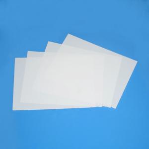
High Insulation 96% 99% Thin Film Al2O3 Aluminum Oxide Ceramic Substrate For PCB
Specification of alumina ceramic substrate
● Material : 99.5% alumina, 99% alumina, 96% alumina, zirconia
optional
● Dimensions: Side length max. 400mm x 300mm, Thickness can be
0.2mm to 20mm
● Additional processing: Precision machining, Laser cutting
● Surface treatment: Fine ground, Well-polished, Metallization,
Glazed
● The checklist of standard size with the stock level in 96%
alumina:
Size (Unit: mm) | Thickness(Unit: mm) | |||
| 132 x 142 | 1.0 | 0.635 | 0.80 | |
| 114 x 114 | 1.0 | 0.635 | 0.80 | 0.385 |
| 109 x 130 | 1.0 | 0.635 | 0.80 | |
| 109 x 109 | 1.0 | 0.635 | 0.80 | |
| 280 x 87 | 0.635 | |||
| 395 x 83 | 1.0 | |||
| 122 x 120 | 1.0 | 0.80 | ||
| 109 x 120 | 1.0 | 0.635 | 0.80 | |
| 138 x 190 | 1.0 | 0.635 | 0.76 | |
| 127 x 127 | 1.0 | 0.635 | ||
| 280 x 240 | 1.0 | 0.635 | ||
Description of alumina ceramic substrate
We offer a great many of aluminum oxides (alumina) ceramic
substrates under rigorous quality control with carefully selected
high purity ceramic materials that ensure stable and consistent
quality and excellent properties.
These alumina substrates have extraordinary properties of
electrical insulation, thermal conductivity, breaking strength and
high-temperature resistance. Furthermore, one of the unique
properties is its surface roughness. We can provide the ceramic
substrate which is excellent in adhesion with a thin film and thick
film metallization due to fine particles.
The main forming method we use is tape-casting, we are dealing with
a variety of selection of thickness from 0.25mm to 20mm. We have
technologies and extensive knowledge about ceramic materials to do
precision processing, like metallization, CNC machining, glazing,
polishing, laser cutting and so on.
The advantages of alumina ceramic substrate:
1.High thermal conductivity, up to 24 W/m.k at 25℃
2.Good thermal shock resistance, greater than 220 T(℃)
3.Good surface roughness, flatness to be 0.05mm
4.High dielectric strength, low dielectric constant and dielectric
loss.
5. Laser cutting or precision machining cutting makes tight
tolerance.
Typical applications of alumina ceramic substrate:
LED packages, Power modules, Substrates for chip resistors, HIC
substrates for heat dissipation, FAX substrates for thermal printer
head, Substrates for automotive parts, Substrates for general thick
film application, Substrates for sensor parts, Substrates for
electronic devices
Why choose us?
★ 10+ Years of manufacturing experience in OEM, ODM ★ Powerful R&D,
mass production capability
★ In-house comprehensive manufacturing types of equipment ★
Rigorous quality control system and processes
★ Surpassing pre-sales and after-sales service ★ Abide all orders
as the first priority
FAQ
Q1. Are you a factory or trading company?
A: We are a manufacturer. You are welcome to visit our factory.
Q2: Do you send a sample to check?
A: Sure, the sample is free and freight collect.
Q3: When will you ship it?
A: If the products are in storage, we'll ship within 48 hours
Q4: When can I get the price?
A: We regularly quote within 24 hours after we get your inquiry. If
you are in urgent need of getting the price.
Please call us or tell us in your email so that we will proceed
with your inquiry as a priority.
Q5: Is it available to provide customized products?
A: We always support custom-made demand as per different materials,
dimensions, and designs.
Q6: How to ensure quality?
A: The dimension out of any batch will be carried out sampling
inspection per international AQL standard. A 100% cosmetic
inspection will be done.
Q7: What other products are you dealing with?
A: We focus on a variety of ceramic tubes, ceramic substrates,
ceramic sheets, textile ceramics besides metalized ceramics.


PCB Ceramic Substrate , Insulation Alumina Substrate Laser Cutted High Accuracy
Inquiry Cart
0