
Add to Cart
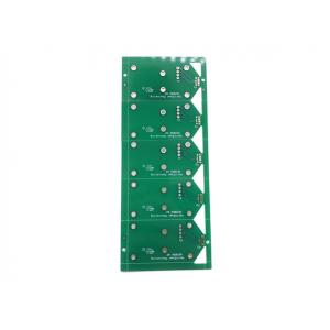
Bare Printed Circuit Board Two Layer Basis OEM Custom 1OZ HASL PCB
ABIS CIRCUITS CO., LTD is a professional PCB manufacturer which is focus on double side, Multilayer and HDI PCB mass production. The company was established in 2006, we have two factories together (audited by UL,ISO9001/14001,SGS,RoHS report), now we dedicated to LED PCB and offer OEM/ODM service for LED products, And all products adhere to IPC Class 2 and IPC Class 3 international PCB standard.
Single-Sided PCB vs. Double-Sided PCB:
What is the difference between single-sided PCBs and double-sided PCBs and how does it affect your business? The single-sided PCB is the original printed circuit board, containing only one layer of conductive material with all the components on one side. They are an extremely popular configuration for printed circuit boards.
Double-sided PCBs are also very popular. The difference is that they use both sides of the board, with a conductive dielectric layer, circuit copper layers and solder mask on both the top and the bottom, connected by vias, so that the traces on the front can communicate with the ones on the back.
Product Details:
1. Rigid, Flex, Rigid-Flexible PCB.
2. Buried/Blind Vias, Via in Pad, Counter Sink Hole, Screw
Hole(Counterbore), Press-fit, Half Hole.
3. HASL lead-free, Immersion Gold/ Silver/Tin, OSP, Gold
plating/finger, Peelable mask,
4. Printed Circuit Boards adhere to IPC Class 2 & 3 international
PCB standard.
5. Quantities range from prototype to medium & big batch
production.
6. 100% E-test
Capacities:
| No. of Layers | 1-20 |
| Max. Board Size | 860*610mm |
| Board Thickness | 0.2-6.0mm |
| Copper Thickness | 0.5OZ-6OZ |
| Material | Various |
| Surface Finish | Various |
| Soldermask | Various |
| Minimum Soldermask Thickness | 0.025mm |
| Minimun Soldermask BridgeDam | 0.15mm |
| Minimum Soldermask Clearance | 0.075mm |
| Peelable Colours | Blue |
| Peelable Minimum Feature | 0.5mm |
| Peelable Maximum Tented Hole | 3.0mm |
| Scoring Angle | 30 Degrees |
| Min. Remaining Thickness | 0.3mm |
| Min. Distance to copper (From center of scoring line) | 0.5mm |
| Min. Track | 0.1mm |
| Min.Gap(TrackTrack,TrackPad,PadPad) | 0.1mm |
| NPTH Min. Drill Size | 0.2mm |
| Plated Drill Size | ± 0.075mm |
| Non-Plated Drill Size | ± 0.05mm |
| Drill Location Tolerance | ± 0.05mm |
| OutlineRouted Slots | ± 0.1mm |
| Line Width/Spacing | ±10% |
| Board Thickness | ±10% |
| Warp and Twist | 0.05% |
| Scoring/V-Cut | ± 5 degrees |
| Scoring Positional Tolerance | ± 0.1mm |
| Aspect Ratio | 10:01 |
Lead Time:
| Board Type | Manufacturing Lead Time |
| Single Sided | 5 – 20 Days dependant on volume |
| PTH | 7 – 25 Days dependant on volume |
| Multilayer | 15 – 30 Days dependant on volume & Technology |
·
| Air Freight Lead Time – 4 Days |
| Sea Freight Lead Time – 30 Days |
| All Far East lead times are subject to customs clearance |
| Premium International shipments can be arranged by DHL, Fedex, UPS or TNT at extra cost |
FAQ:
Q1:What's your Aluminum board Thermal Conductivity?
A: Normally 0.8-3W/m.K. If you have special demands please feel
free contact us
Q2:Is my PCB file safe if I send it to you for manufacturing?
A: We respect customer's design authority and will never
manufacture PCB for someone else without your permission. NDA is
acceptable.
Q3:What is your testing policy and how you control the quality?
A: For sample, usually tested by flying probe; for PCB Volume over
3 square meters, usually tested by fixture, this will be more
faster. Due to there's many steps to PCB production, we usually do
inspection after every step.
Q4: What's your shipping way ?
A: 1. We have our own forwarder to ship goods by DHL, UPS, FEDEX,
TNT,EMS.
2. If you have your own forwarder, we can cooperate with them.
Q5: What is your certificate?
A: ISO9001:2008, ISO14001: 2004, UL, SGS,RoHS report.
Q6: What files should we offer?
A: If only need PCB, please provide Gerber File and manufacturing
specifications; If need PCBA,Please provide Gerber File,
Manufacturing specification, BOM list and Pick & Place/XY file.
Q7: Can I get a sample?
A: Yes, It's reasonable to get a sample to test our quality at
first.
Q8: Does ABIS CIRCUITS bevel gold fingers?
A: Yes. A standard 45-degree bevel, also bevel at 15 or 30 degrees
upon request. For multi-layer board, please ensure there is
adequate back set for the bevels.
Q9: Why choose us?
A: With ABIS, customers significantly and effectively reduce their
global procurement costs. Behind each service provided by ABIS, is
hidden a cost saving for customers.
Products We Made:
Manufacturer Equipment:


