
Add to Cart
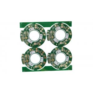
Fast Turn Small Prototype Runs Gerber Files Of PCB Electronics PCB Design
Our service:
High speed, multi layer digital PCB designs – Bus routing,
differential pairs, matched lengths.
Extensive RF and analog design experience (printed antennas, guard
rings , RF shields…)
Signal integrity issues to meet your digital design needs (tuned
traces, diff pairs…)
PCB Layer management for signal integrity and impedance control
DDR2, DDR3, DDR4, SAS and differential pair routing expertise
High density SMT designs (BGA, uBGA, PCI, PCIE, CPCI…)
Flex PCB designs of all types
Low level analog PCB designs for metering
Ultra low EMI designs for MRI applications
Complete assembly drawings
In-Circuit Test data generation (ICT)
Drill, panel and cutout drawings designed
Professional fabrication documents created
PCB capability:
| Product Name | Electronics PCB Design |
| Type | Rigid |
| Material | FR4, CEM1, CEM3, High Frequency Board, |
| Layer | 1,2,4,6...20Layer |
| Shape | Retangular, Round, Slots, Cutouts, Complex, Irregular |
| Cutting | Shear, V-score, Tab-routed |
| Board Thickness | 0.2-4mm, regular 1.6mm |
| Copper Thickness | 0.5-4oz, regular 1oz |
| Silk Screen | White, Black, etc. |
| Silk Screen Min Line Width | 0.006" or 0.15mm |
| Min Trace/Gap | 0.1mm or 4mils |
| Min Drill Hole Diameter | 0.01",0.25mm or 10mils |
| Surface Finish | HASL, ENIG, OSP, etc. |
Company Attributes:
Full turnkey electronic engineering solutions that cover your
project from concept to production
Military, space, smart home,medical, automotive and commercial
applications
Highly knowledgeable team of electronic engineers and PCB designers
Experts in RF PCB Design, high speed digital PCB design and
microwave electronic design
Member of IPC designer's council with PCB design certification
Solid PCB manufacturing knowledge for superior designs
Great communication with customers and comprehensive online design
reviews
Exceptional turn time on projects to help meet customer deadlines
Complete confidentiality of your projects and IP
Competitive prices on of our all services
Customers worldwide!
Expert PCB sample Assembly services for Military, space, smart home,medical, automotive, commercial and ect:
Shenzhen Yideyi Technology Co., Ltd can simulate your design before going to PCB layout to make sure it will work as expected
FAQ:
Q1. How can we ensure our information should not let third party to
see our design?
We are willing to sign NDA effect by customer side local law and
promising to keep customers date in high confidential level in all
projects.
Q2. How long does it take for PCB and PCBA Quote ?
PCBs quotation within 2 hours can finished the PCBA depend on the
components
quantity,if simple, within 6 hours can finished,once complex and
more,the 12- 36 hours
can be finished.
Q3. Please note that the following detail will speed up evaluation:
Material:
Board thickness:
Copper thickness:Surface finish:
Solder mask color:
Silkscreen color:
Q4. How about the delivery?
Normally, for sample order, our delivery is about 5 days.For small
batch, our delivery is about 7 days.
For mass production batch, our delivery is about 10 days.
But that depends on the real condition when we get your order.
If your order is urgently please contact us directly ,we will
priority to deal it and do ourbest to give you satisfied delivery
time.
Q5. With payment terms do we accept?
For sample order or small batch, we suggest you to use Pay-pal and
Western Union.For mass production batch, we suggest you to use T/T.
Q6. How can we guarantee you receive an good quality product?
For PCB, we will use Flying Probe Test, E-test etc. for it.
For PCBA, we need you to offer us a method or test fixture for the
function test.Before that, our inspectors will use microscope and
X-ray to check the IC footwelding or bad solder etc.


