
Add to Cart
InP wafer ( Indium phosphide )
We provides high quality single crystal InP wafer ( Indium phosphide ) to micro-electronic ( HBT/ HEMT ) and opto-electronic industry ( LED / DWDM / PIN / VCSELs ) in diameter up to 3 inch . Indium phosphide ( InP ) crystal is formed by two elements , Indium and Phosphide , growth by Liquid Encapsulated Czochralski ( LEC ) method or VGF method . InP wafer is an important semiconductor material which have superior electrical and thermal properties , compared to silicon wafer and GaAs wafer , InP wafer has higher electron mobility ,higher frequency , low power consumption , higher thermal conductivity and low noise performance . We can provide epi ready grade InP wafer for your MOCVD & MBE epitaxial application .Please contact us for more product information .
III-V Compound Wafer
We provides a wide range of compound wafer including GaAs wafer, GaP wafer, GaSb wafer, InAs wafer, and InP wafer .
Electrical and Doping Specification
Product Specification
| Growth | LEC / VGF |
|---|---|
| Diameter | Ø 2" / Ø 3" / Ø 4" |
| Thickness | 350 um ~ 625 um |
| Orientation | <100> / <111> / <110> or others |
| Off orientation | Off 2° to 10° |
| Surface | One side polished or two sides polished |
| Flat options | EJ or SEMI. Std . |
| TTV | <= 10 um |
| Bow / Warp | <= 20 um |
| Grade | Epi polished grade / mechanical grade |
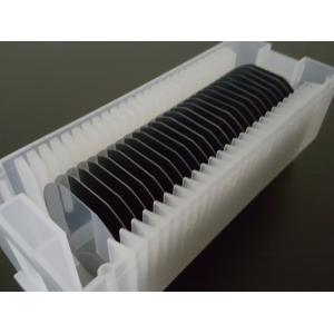
| Package | Single wafer container |

