Add to Cart
Small Hole Size Multi-Layer Printed Circuit Board Production For High-Density Designs
Multilayer PCB Fabrication is a manufacturing process that produces multi-layer printed circuit boards (PCBs) from a variety of materials. The most common materials used in the fabrication process include FR4, high TG FR4, halogen-free, and Rogers materials. Through this process, multilayer PCBs are manufactured to meet the required geometry, electrical performance, and other specifications. The process involves the use of advanced equipment and techniques to achieve high precision and accuracy.
When it comes to multilayer PCB fabrication, the minimum line width that can be achieved is 0.1mm and the minimum hole size is 0.2mm. In addition, the board thickness can range from 0.2mm to 3.2mm and various surface finishes can be applied such as HASL, ENIG, OSP, immersion silver, and immersion tin.
In addition to the fabrication process, multilayer PCB component assembly is also possible. This includes processes such as component assembly, soldering, and conformal coating. All of these processes are carried out in an automated and controlled environment to ensure high quality and reliability.
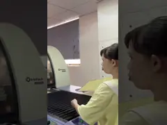
The multilayer PCB manufacturing process is highly complex and requires the use of advanced equipment and techniques to ensure the highest levels of quality and reliability. As such, it is essential that the process is carried out by experienced professionals who have the necessary expertise and knowledge to ensure that the final product meets the customer's requirements.
| Property Name | Property Value |
|---|---|
| Board Thickness | 0.2-3.2mm |
| Impedance Control | Yes |
| Layer Count | 2-20 |
| Min. Hole Size | 0.2mm |
| Min. Line Spacing | 0.1mm |
| Copper Thickness | 1-4oz |
| Material | FR4, High TG FR4, Halogen Free, Rogers, Etc. |
| Min. Line Width | 0.1mm |
| Silkscreen Color | White, Black, Yellow, Etc. |
| Solder Mask Color | Green, Blue, White, Black, Red, Etc. |
| Production Process | Multi-Level Printed Wiring Board Creation, Multi-Layer PCB Component Assembly |
JIETENG's Multi-Level Printed Wiring Board Creation and Multi-Layer Printed Circuit Board Production is a reliable and cost-effective solution for all of your circuit board needs. The product is made in China and features HASL, ENIG, OSP, Immersion Silver, Immersion Tin, and other surface finishes. Impedance control is also available. The product comes in layer counts from 2 to 20, and features a minimum line width of 0.1mm. Additionally, silkscreen colors such as white, black, yellow, and other options are available. This product is perfect for creating reliable and cost-effective multi-level printed wiring boards and multi-layer printed circuit boards.
Brand Name: JIETENG
Model Number: PCB circuit board
Place of Origin: China
Impedance Control: Yes
Material: FR4, High TG FR4, Halogen Free, Rogers, Etc.
Layer Count: 2-20
Min. Line Spacing: 0.1mm
Min. Line Width: 0.1mm
We offer Multi-Layer PCB Component Assembly, Multi-Level Printed Circuit Board Fabrication, Multi-Layer PCB Manufacturing.
We offer a comprehensive range of technical support and services for Multilayer PCB Fabrication. Our team of experienced engineers and technicians can provide advice on product design, engineering, and fabrication.
We also provide a full range of services for prototyping and production, including PCB layout, fabrication, assembly, testing, and troubleshooting. Our services are tailored to meet the specific requirements of each customer, and our engineers are available to work with you to ensure that your project meets the highest standards.
Our team is committed to providing the highest level of quality, service, and support to ensure that your Multilayer PCB Fabrication project is a success.
Packaging and Shipping for Multilayer PCB Fabrication:
To ensure that the product arrives in excellent condition, we use quality packaging materials for our multilayer PCB fabrication orders.
Our typical packaging includes a durable corrugated box with foam cushioning for the PCBs. We also use a moisture-proof bag inside the box to keep the product dry. For international shipping, we also add an extra layer of cardboard and bubble wrap for extra protection.
We use a reliable courier service for all our shipments. Depending on the location, we use both air and sea freight.