Add to Cart
SMT PCBA Printed Circuit Board Assembly ,Custom Pcba Assembly ISO/UL
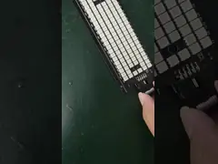
This 4 layers multilayer PCBA is assembly with SMT and DIP. The
bare printed circuit board used is 1.6 mm thick and with Leadfree
HASL surface treatment, make the pcb more eco-friendly. The outer
and inner of the PCB is both 1 Oz / 35 µm.
Files Requested For PCB Assembly Quotation
---In order to provide you with the most efficient and accurate
quote on manufacturing the requested unit, we ask that you provide
us with the following information.
1. Gerber file,PCB file,Eagle file or CAD file are all acceptable
2. A detailed bill of materials (BOM)
3. Clear pictures of PCB or PCBA sample for us
4. Quantity and delivery required
5. Test method for PCBA to guarantee 100% good quality products.
6. Schematics file for PCB design if need to do function test.
7. A sample if available for better sourcing
8. CAD files for enclosure manufacturing if required
9. A complete wiring and assembly drawing showing any special
assembly instructions if required
Shinelink kinds PCBA product
Technical Support
- Professional Surface-mounting and Through-hole soldering
Technology
- Various sizes like 1206,0805,0603 components SMT technology
- ICT(In Circuit Test),FCT(Functional Circuit Test) technology.
- PCB Board Assembly With UL,CE,FCC,Rohs Approval
- Nitrogen gas reflow soldering technology for SMT.
- High Standard SMT&Solder Assembly Line
- High density interconnected board placement technology capacity.
PCB Assembly Capabilities
Turnkey PCBA | PCB+components sourcing+assembly+package |
Assembly details | SMT and Thru-hole, ISO lines |
Lead Time | Prototype: 15 work days. Mass order: 20~25 work days |
Testing on products | Flying Probe Test, X-ray Inspection, AOI Test, functional test |
Quantity | Min quantity: 1pcs. Prototype, small order, mass order, all OK |
Files we need | PCB: Gerber files(CAM, PCB, PCBDOC) |
Components: Bill of Materials(BOM list) | |
Assembly: Pick-N-Place file | |
PCB panel Size | Min size: 0.25*0.25 inches(6*6mm) |
Max size: 20*20 inches(500*500mm) | |
PCB Solder Type | Water Soluble Solder Paste, RoHS lead free |
Components details | Passive Down to 0201 size |
BGA and VFBGA | |
Leadless Chip Carriers/CSP | |
Double-sided SMT Assembly | |
Fine Pitch to 0.8mils | |
BGA Repair and Reball | |
Part Removal and Replacement | |
Component package | Cut Tape,Tube,Reels,Loose Parts |
PCB assembly | Drilling-----Exposure-----Plating-----Etaching & Stripping-----Punching-----Electrical Testing-----SMT-----Wave Soldering-----Assembling-----ICT-----Function Testing-----Temperature & Humidity Testing |
PCBA Picture