High Purity un-doped Silicon Carbide sic Wafer , 6Inch 4H-Semi Sic Silicon Carbide Substrate
Brand Name:zmsh
Model Number:sic- 6inch
Minimum Order Quantity:1pcs
Delivery Time:15days within
Place of Origin:china
Price:by case
Contact Now
Add to Cart
Verified Supplier
Location:
Shanghai Shanghai China
Address:
Room.1-1805,No.1079 Dianshanhu Road,Qingpu Area Shanghai city, China /201799
Supplier`s last login times:
within 13 hours
Product Details
Company Profile
Product Details
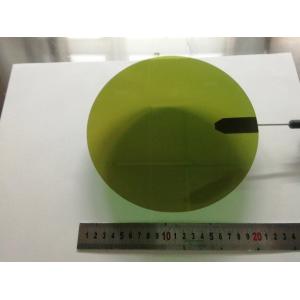
6inch sic substrates, 4h-n,4H-SEMI,sic ingot sic crystal ingots sic crystal block sic semiconductor substrates,High purity silicon carbide
SiC Wafer
SiC crystal are cutted into slices, and polishing, the SiC wafer comes. For specification and details, please visit below page.
SiC crystal growth
Bulk crystal growth is the technique for fabrication of single crystalline substrates , making the base for further device processing.To have a breakthrough in SiC technology obviously we need production of SiC substrate with a reproducible process.6H- and 4H- SiC crystals are grown in graphite crucibles at high temperatures up to 2100—2500°C. The operating temperature in the crucible is provided either by inductive (RF) or resistive heating. The growth occurs on thin SiC seeds. The source represents polycrystalline SiC powder charge. The SiC vapor in the growth chamber mainly consists of three species, namely, Si, Si2C, and SiC2, which are diluted by carrier gas, for example, Argon. The SiC source evolution includes both time variation of porosity and granule diameter and graphitization of the powder granules.
SiC epi wafer
We can cost-effectively produce very high quality epitaxial
structures for device or testing purposes.The silicon carbide (SiC)
epitaxial wafer poses many advantages in comparision with
conventional Si wafers, We can offer epi layer in very large range
of doping concentration 1E15/cm3 from low 1014 to 1019 cm-3 for
more information.
SiC Crystal Structure
SiC Crystal has many different crystal structures,which is called polytypes.The most common polytypes of SiC presently being developed for electronics are the cubic 3C-SiC, the hexagonal 4H-SiC and 6H-SiC, and the rhombohedral 15R-SiC. These polytypes are characterized by the stacking sequence of the biatom layers of the SiC structure
sic crystal defects
Most of the defects which were observed in SiC were also observed in other crystalline materials. Like the dislocations, stacking faults (SFs), low angle boundaries (LABs) and twins. Some others appear in materials having the Zing- Blend or the Wurtzite structure, like the IDBs. Micropipes and inclusions from other phases mainly appear in SiC.
SiC crystal application
Many researchers know the general SiC application:III-V Nitride Deposition;Optoelectronic Devices;High Power Devices;High Temperature Devices;High Frequency Power Devices.But few people knows detail applications, We list some detail
material application and advantagement
• Low lattice mismatch
• High thermal conductivity
• Low power consumption
• Excellent transient characteristics
• High band gap
Applications:
• GaN epitaxy device
• Optoelectronic device
• High frequency device
• High power device
• High temperature device
• Light emitting diodes
| Property | 4H-SiC, Single Crystal | 6H-SiC, Single Crystal |
| Lattice Parameters | a=3.076 Å c=10.053 Å | a=3.073 Å c=15.117 Å |
| Stacking Sequence | ABCB | ABCACB |
| Mohs Hardness | ≈9.2 | ≈9.2 |
| Density | 3.21 g/cm3 | 3.21 g/cm3 |
| Therm. Expansion Coefficient | 4-5×10⁻⁶/K | 4-5×10⁻⁶/K |
| Refraction Index @750nm | no = 2.61 ne = 2.66 | no = 2.60 ne = 2.65 |
| Dielectric Constant | c~9.66 | c~9.66 |
| Thermal Conductivity (N-type, 0.02 ohm.cm) | a~4.2 W/cm·K@298K c~3.7 W/cm·K@298K | |
| Thermal Conductivity (Semi-insulating) | a~4.9 W/cm·K@298K c~3.9 W/cm·K@298K | a~4.6 W/cm·K@298K c~3.2 W/cm·K@298K |
| Band-gap | 3.23 eV | 3.02 eV |
| Break-Down Electrical Field | 3-5×10⁶V/cm | 3-5×10⁶V/cm |
| Saturation Drift Velocity | 2.0×10⁵m/s | 2.0×10⁵m/s |
2. Material Size describtion
3. products
FAQ
Q:How about the delivery time and quality.
A: We have strict quality inspection system. and Delivey by DHL,
Fedex, EMS by your require
Q: Are you a trading company or a factory?
A: We have a wafer process factory, which can reduce all cost we
can control.
Q: What’s your main products?
A: There are saphire wafer,sic,Quartz wafer .We can also produce
special shape
products according to your drawing.
Q: What’s your advantage?
A:
1. Price. We are not only a trading company, so we can get the most competitive price for you and ensure our products quality &price as
well as the delivery time.
2. Technology. Our company has 5-year experience on producing wafer
& optical products.
3. After-sales service. We can be responsible for our quality.
Shipment & package
Thanks~~~


High Purity un-doped Silicon Carbide sic Wafer , 6Inch 4H-Semi Sic Silicon Carbide Substrate
Inquiry Cart
0