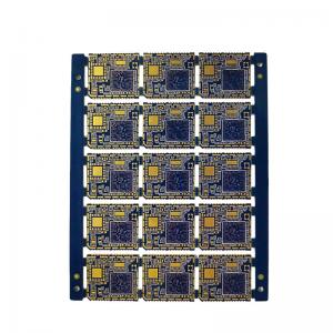
Oem EM528K Assembly Pcb Assembly Smt Circuit Board
Brand Name:TOPCBS
Certification:UL94V0
Model Number:1.0mm thermal bar 12 Anylayer HDI / Optical module board
Minimum Order Quantity:Negotiation
Delivery Time:10-14working days
Payment Terms:T/T
Contact Now
Add to Cart
Active Member
Location:
Suzhou Jiangsu China
Address:
Room 301, Building 1, Shahu Science and Technology Park, SIP, SUZHOU City,Jiangsu Province,P.R.C
Supplier`s last login times:
within 22 hours
Product Details
Company Profile
Product Details
Oem Assembly Pcb Assembly Smt Circuit Board
A well designed circuit board means:
· A reduction in production problems
· Improved quality control
· Reduced costs
· Reduced manufacturing times
1 . Descriptions:
What is a HDI PCB?
HDI stands for High Density Interconnector. A circuit board which has a higher wiring density per unit area as opposed to conventional board is called as HDI PCB. HDI PCBs have finer spaces and lines, minor vias and capture pads and higher connection pad density. It is helpful in enhancing electrical performance and reduction in weight and size of the equipment. HDI PCB is the better option for high-layer count and costly laminated boards.
Regarding the electrical needs of high-speed signal, the board
should have various features i.e. high-frequency transmission
capability, impedance control, decreases redundant radiation, etc.
The board should be enhanced in the density because of the
miniaturization and arrays of the electronic parts. In addition, to
the result of the assembling techniques of leadless, fine pitch
package and direct chip bonding, the board is even featured with
exceptional high-density.
Innumerable benefits are associated with HDI PCB, like high speed,
small size and high frequency. It is the primary part of portable
computers, personal computers, and mobile phones. Currently, HDI
PCB is extensively used in other end user products i.e. as MP3
players and game consoles, etc.
2 . Specifications:
| Item | Specification | |
| 1 | Numbr of Layer | 1-18Layers |
| 2 | Material | FR-4,FR2.Taconic,Rogers, CEM-1 CEM-3,ceramic , crockery Metal-backed Laminate |
| 3 | Surface Finish | HASL(LF), Gold plating, Electroless nickel immersion gold, Immersion Tin, OSP(Entek) |
| 4 | Finish Board Thickness | 0.2mm-6.00 mm(8mil-126mil) |
| 5 | Copper Thickness | 1/2 oz min;12 oz max |
| 6 | Solder Mask | Green/Black/White/Red/Blue/Yellow |
| 7 | Min.Trace Width & Line Spacing | 0.075mm/0.1mm(3mil/4mil) |
| 8 | Min.Hole Diameter for CNC Driling | 0.1mm(4mil) |
| 9 | Min.Hole Diameter for punching | 0.9mm(35mil) |
| 10 | Biggest panel size | 610mm*508mm |
| 11 | Hole Positon | +/-0.075mm(3mil) CNC Driling |
| 12 | Conductor Width(W) | 0.05mm(2mil)or; +/-20% of original artwork |
| 13 | Hole Diameter(H) | PTH L:+/-0.075mm(3mil); Non-PTH L:+/-0.05mm(2mil) |
| 14 | Outline Tolerance | 0.125mm(5mil) CNC Routing; +/-0.15mm(6mil) by Punching |
| 15 | Warp & Twist | 0.70% |
| 16 | Insulation Resistance | 10Kohm-20Mohm |
| 17 | Conductivity | <50ohm |
| 18 | Test Voltage | 10-300V |
| 19 | Panel Size | 110×100mm(min);660×600mm(max) |
| 20 | Layer-layer misregistration | 4 layers:0.15mm(6mil)max; 6 layers:0.25mm(10mil)max |
| 21 | Min.spacing between hole edge to circuity pqttern of an inner layer | 0.25mm(10mil) |
| 22 | Min.spacing between board oulineto circuitry pattern of an inner layer | 0.25mm(10mil) |
| 23 | Board thickness tolerance | 4 layers:+/-0.13mm(5mil); 6 layers:+/-0.15mm(6mil) |
| 24 | Impedance Control | +/-10% |
| 25 | Different Impendance | +-/10% |
3. Advantages:
The most common reason for using HDI technology is a significant increase in packaging density. The space obtained by finer track structures is available for components. Besides, overall space requirements are reduced will result in smaller board sizes and fewer layers.
Usually FPGA or BGA are available with 1mm or less spacing. HDI technology makes routing and connection easy, especially when routing between pins.


Oem EM528K Assembly Pcb Assembly Smt Circuit Board
Inquiry Cart
0