High Density Interconnect Hdi Pcb Burn In Test Procedure 0.25 Pitch 12Layer
Brand Name:TOPCBS
Certification:UL94V0
Model Number:BIB and test Boards
Minimum Order Quantity:Negotiation
Delivery Time:10-14working days
Payment Terms:T/T
Contact Now
Add to Cart
Active Member
Location:
Suzhou Jiangsu China
Address:
Room 301, Building 1, Shahu Science and Technology Park, SIP, SUZHOU City,Jiangsu Province,P.R.C
Supplier`s last login times:
within 22 hours
Product Details
Company Profile
Product Details
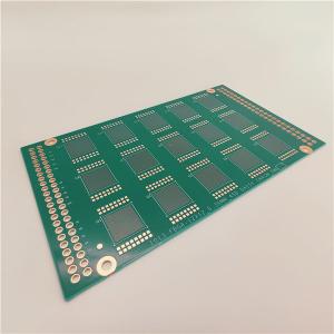
0.25 pitch 12Layer HDI PCBs for Burn in boards and semiconductor Test boards / thin board
- Reduced product development time
- Increased customer confidence
- 100% product quality and reliability
- A forecast life expectancy
- Reduced circuit board manufacturing costs
- Increased profitability
- Reduced after sales service
1 . Descriptions:
What is a BIB ?
A burn-in board is a printed circuit board that is used in the burn-in process. The components added to the board are stressed using extreme heat to highlight any failures. Once the stress tests have been completed engineers will analyse the results to make sure everything is working within the correct parameters.
2 . Specifications:
| Name | 0.25pitch 12Layer HDI PCBs for Burn in boards and semiconductor Test boards |
| Number of Layers | 12 |
| Quality Grade | IPC 6012 Class 2,IPC 6012 Class 3 |
| Material | IT180 |
| Thickness | 0.7mm |
| Min Track/Spacing | 75um/75um |
| Min Hole Size | Laser 75um |
| Solder Mask | Green |
| Silkscreen | White |
| Surface Finish | Immersion gold + OSP |
| Finished Copper | 12um |
| Production time | 10-21 working days |
| Lead time | 2-3 days |


High Density Interconnect Hdi Pcb Burn In Test Procedure 0.25 Pitch 12Layer
Inquiry Cart
0