
Add to Cart
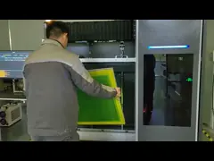
Laser Direct Imaging Printed Circuit Board (LDIPCB) is a reliable
and widely used technology for the manufacture of Printed Circuit
Boards (PCB). It makes use of laser imaging to transfer a PCB
design onto the circuit board. This technology offers the
advantages of high accuracy, low cost and fast turnaround time. The
effective exposure area of LDIPCB is 620x720mm, with an alignment
accuracy of ±12um, and line width tolerance of ±10%. It is
applicable for solder mask and outer processes, and supports file
formats including Gerber, ODB++ and Cals.
LDIPCB provides the highest level of precision and accuracy for PCB
manufacturers, enabling them to produce high-quality and reliable
PCBs with a quick turnaround time. It eliminates the need for
complex and costly processes, such as silkscreen printing and
etching. This makes it an ideal choice for PCB manufacturing, and
is widely used in a variety of industries, including consumer
electronics, automotive, and medical.
Laser Direct Imaging Printed Circuit Board (LDIPCB) is the perfect
solution for those looking for a reliable, high-quality and
cost-effective PCB manufacturing solution. It offers superior
accuracy and precision, with no need for complex and costly
processes. It is an ideal choice for PCB manufacturers who need to
produce high-quality and reliable PCBs with a quick turnaround
time.
| Parameter | Specification |
| Solder Mask Color | Fixed Scale/ Auto Scale / Interval Scale / Partition Alignment |
| Laser Power | Mixing Wave Total Power 512W |
| Line width tolerance | ±10% |
| Alignment accuracy | ±12um |
| File format | File Format |
| Application | PCB,HDI,FPC |
| Effective exposure area | 620x720mm(24 |
| Board thickness | 0.5~3.5mm |
| Scale mode | White, Black, Yellow, Etc. |
| Solder mask ink | 30s@600x500mm(24 |
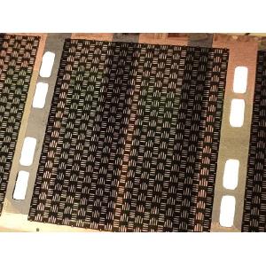
GIS DPX820SM Laser Direct Imaging Print Board has become a popular
choice for many applications due to its precision and reliability.
This product is made by Suzhou, China and usually used in Solder
Mask, Outer process. It features 50/75μm solder bridge/solder
opening and 30s@600x500mm solder mask ink. The alignment method is
PAD with diameter of 0.5~3.0mm and File Format for the files.
GIS DPX820SM Laser Direct Imaging Printed Board is highly suitable
for applications which require high precision and reliability. It
is widely used in the automotive, aviation, and aerospace
industries. It is also used in medical, industrial, and consumer
electronics. With its high accuracy and performance, this product
can be used for the production of high-precision products such as
PCBs, electronic components, and other components.
GIS DPX820SM Laser Direct Imaging Circuit Board is the perfect
choice for manufacturers who need to produce complex circuit boards
with high accuracy. Its advanced laser direct imaging technology
makes it possible to produce extremely precise components. It also
offers great flexibility in terms of design. Its high speed and
high resolution make it the ideal choice for complex circuitry and
complex components.
GIS DPX820SM Laser Direct Imaging Print Board is the ideal choice
for those who need a reliable and accurate product for their PCB
manufacturing needs. With its superior quality and performance,
this product can provide an efficient and cost-effective solution
for any application. Whether you are looking for a product to use
in soldering, outer process, or any other application, GIS DPX820SM
Laser Direct Imaging Printed Board is the perfect choice.
GIS Laser Direct Imaging Printed Circuit Board (DPX820SM) is a reliable and robust printed circuit board solution. It is produced in Suzhou, China and features scale mode options such as white, black and yellow. It also has 30s@600x500mm(24 solder mask ink and PAD alignment method (diameter: 0.5~3.0mm). The board thickness range is 0.5~3.5mm and the line width tolerance is ±10%.
For more information about GIS Laser Direct Imaging Printed Circuit Board (DPX820SM), please contact us.
Laser Direct Imaging (LDI) PCB technology provides customers with
technical support and services to ensure the quality and
reliability of their products.
Technical Support: Our experienced engineers are always available
to assist customers with any technical questions they may have. We
can provide technical advice and recommendations to ensure that
customers’ products are of the highest quality. We also provide
on-site support when necessary.
Services: Our services include product testing, troubleshooting and
repair. We use the latest testing equipment and techniques to
ensure that our customers’ products meet their requirements. We
also offer repair services when necessary. We strive to provide the
best possible service to our customers.
Packaging and Shipping for Laser Direct Imaging PCB:
The Laser Direct Imaging PCB will be packed in a strong cardboard
box with protective packaging materials such as bubble wrap and
foam to prevent any potential damage during transportation. The box
will be sealed with strong adhesive tape. The package will then be
shipped via a reliable courier with tracking capability.