
Add to Cart
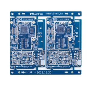
Multilayer Printed Circuit Board 6 Layer Printed Circuit Board Small Line Space And Gap Impedance Control
6 Layer Rigid PCB with small line space and gap
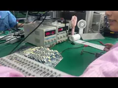
HSX Circuit covers over 5,000 PCB products monthly, from single layer to 32L FR-4 PCB, from IMS PCB,HDI Boards, to high frequency PTFE boards and Rigid-flex boards. We provides flexible quick turn production services (12 hours to72 hours), as well as small volume to big volume PCB manufacturing.
Products are widely used in high-tech fields such as communications, power supplies, computer networks, digital products, industrial control, science and education, medical devices, and aerospace, and so on.
Max layers: 32layer (≥20 layer needs to review the capability)
Max finish panel size: 740* 500 MM(>600 MM needs to review capability)
Min finish panel size: 5 * 5mm
Raw material: PI +FR4,FR4, Rogers, AI and so on
PCB finished board thickness: 0.2~4.0mm(<0.2 mm,>4 mm needs to review) (Board thickness ≤ 0.6mm,do not
apply for HASL surface)
Copper thickness of inner and outer base copper: Min 0.3/0.5oz,Max 3oz, advance 4-6oz
Finished outer copper: 6oz
Bow and twist: 0.075%
Min. hole size: 0.15mm(<0.15 mm needs to review the capability)
HDI Min drill hole: 0.08-0.10MM
PCB track/gap: 3mil(0.075mm)
PCB outline: Routing/V-CUT/Punching
Solder mask thickness: standard 15-20um; Advanced: 35um
Min solder mask bridge width: green 4mil,other colour 4.8mil
Solder mask plugged holes: 0.1-0.5mm
The color of solder mask: green,matt green,blue,matt blue,black,matt black,yellow,red,white, and so on
PCB silkscreen: White, Black and so on
Peelable mask thickness: 500-1000um
Oxidation film of OSP: 0.2-0.5um
| ||||||||||||||||||||||||||||
FAQ:
Q1:Are you a factory or trade company?
A: Yes, we are the factory, we have independent quick turn
prototype PCB manufacturing & big volume PCB production lines.
Q2:How about your PCB factory production capacity?
A: Our monthly production capacity is 50,000 square meter/month and
5000types/month.
Q3:If we have no PCB file/Gerber file, only have the PCB sample,can
you produce it for me?
A: Yes,we could help you to clone the PCB. Just send the sample PCB
to us, we could clone the PCB design and work out it.
Q4:How will you usually ship the PCB?
A: Usually for small packages, we will ship the boards by
DHL,UPS,FedEx door to door service, we could use your shipping
account to do collection or use our account to ship in DDU (import
duty unpaid) delivery term.
For heavy goods more than 300kg, we may ship your PCB boards by
ship or by air to save freight cost. Of course, if you have your
own forwarder, we may contact them for dealing with your shipment.
Q5:What is your standard lead time for production?
A: Sample/prototype(less than 3sqm):
1-2 Layers: 3 to 5working days (fastest 24hours for quick turn
services)
4-8 Layers: 7~12 working days (fastest 48hours for quick turn
services)
Mass production (less than 200sqm):
1-2 Layers:7 to 12 working days
4-8 Layers:10 to 15 working days