
Add to Cart
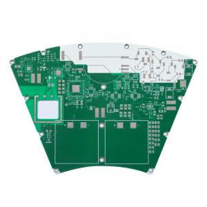
High TG Green Ceramic PCB Board OSP HASL Semiconductor Microelectronics
Ceramic PCB Board Green Ceramic PCB Ceramic Base Material High TG Semiconductor And Microelectronic
Green Ceramic PCB Board
Ceramic PCB have good high-frequency and electrical performance, and have high thermal conductivity, excellent chemical and thermal stability. Excellent corrosion resistance, it widely used in semiconductor and microelectronic circuit packaging pcb, High-brightness Led chip carrier board, automotive electronics and lighting components, high-power electronic component heat dissipation materials, etc.
Ceramic PCBs provide best source of reacting point for printed circuits due to two reasons, high thermal conductivity and low coefficient of thermal expansion (CTE). The ceramic PCB is highly unique and useful because it is a complete replacement of traditional printed circuit boards having simple structure and increased performance.
Characteristics of Ceramic PCB:
1. Ceramic printed circuit boards are excellent heat conductors.
2. Ceramic circuit boards are not easily eroded by chemicals.
3. Ceramic PCBs provide a high level of mechanical compatibility.
4. High-density outlining is simple on ceramic boards.
5. Their CTA component compliance is excellent.
| Items | Normal standard |
| Material | FR-4;High TG FR-4; Ceramic base material |
| Layer NO. | 1-20 |
| Board Size | 50mm*50mm-560mm*640mm |
| Board Thickness | 0.4mm-4.0mm |
| Thickness Tolerance | ±10% |
| Min Hole Size | 0.15mm |
| Copper Thickness | 18um-105um |
| Copper Plating hole | 18um-30um |
| Min Trace Width | 0.1mm |
| Min Space Width | 0.1mm |
| Solder Mask Color | green;blue;black;red... |
| Surfae | Immersion gold, LF-HASL, OSP... |
| Outline profile | CNC; V-CUT; Punching |
| Impedance Control | ±10% |
| certificate | ISO9001 |
FAQ:
Q1:Are you a factory or trade company?
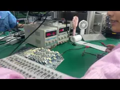
A: Yes, we are the factory, we have independent quick turn
prototype PCB manufacturing & big volume PCB production lines.
Q2:What kind of PCB file format can you accept for production?
A: Gerber, PROTEL 99SE, PROTEL DXP, POWER PCB, CAM350, ODB+(.TGZ)
Q3:Are my PCB files safe when I submit them to you for
manufacturing?
A: We respect customer's copyright and will never manufacture PCB
for someone else with your files unless we receive written
permission from your side, nor we'll share these files with any
other 3rd parties. And we could sign NDA with client if necessary.
Q4:If we have no PCB file/Gerber file, only have the PCB sample,can
you produce it for me?
A: Yes,we could help you to clone the PCB. Just send the sample PCB
to us, we could clone the PCB design and work out it.
Q5:What is your standard lead time for PCB?
A: Sample/prototype(less than 3sqm):
1-2 Layers: 3 to 5working days (fastest 24hours for quick turn
services)
4-8 Layers: 7~12 working days (fastest 48hours for quick turn
services)
Mass production (less than 200sqm):
1-2 Layers:7 to 12 working days
4-8 Layers:10 to 15 working days
Q6:What payment do you accept ?
A: Wire Transfer(T/T) or Letter of Credit(L/C) or Paypal(only for
small value less than 500usd)