
Add to Cart
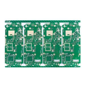
Impedance Control HDI PCB Board 1.2mm 4mil Mobile Phone PCB
HDI PCB Board HDI Buried Vias And Blind Vias Hdi Board Impedance Control Mobile Phone PCB Board
6L 1+N+1 HDI Boards
HDI PCB are abbreviation of high density interconnect printed circuit boards, they are characterized by finer lines, closer spaces, and more dense wiring.
High-density interconnect (HDI) PCBs are characterized by finer lines, closer spaces, and more dense wiring. They have a faster connection while reducing the size of a project. Normally, these boards also feature blind and buried vias, laser ablated microvias, sequential lamination, and via in-pads. A HDI board can house the functionality of the previous boards used.
For HDI boards own higher circuit density than traditional circuit boards, its designs can include smaller through holes and capture pads, and also higher connection pad density. They are widely used to reduce the weight and overall dimensions of products, as well as to enhance the electrical performance of the device.
HDI boards are applied to wide range of industries, like digital devices, smartphones and tablets, automobiles, aircraft and other vehicles products.
| Circuit board Layer count: | 6L | Circuit board laminate: | FR4 S1000-2 TG170 |
| Layer Copper thick: | 1/1/1/1/1/1OZ | Board thickness: | 1.2MM |
| Smallest hole size: | 0.25mm | Smallest PCB track/gap: | 6/4mil |
| Solder mask color: | TAIYO Green | Silk screen color: | White |
| PCB surface finished: | Immersion Gold | Board profile: | Routing/V-CUT |
| PCB Board Application: | communications | ||
| Requesting Special requirement: | HDI Buried vias and blind vias, one step stack up /impedance control/resin filled and plated over | ||
Q1:Are you a factory or trade company?
A: Yes, we are the factory, we have independent quick turn
prototype PCB manufacturing & big volume PCB production lines.
Q2: What kind of PCB file format can you accept for production?
A: Gerber, PROTEL 99SE, PROTEL DXP, POWER PCB, CAM350, ODB+(.TGZ)
Q3: Are my PCB files safe when I submit them to you for
manufacturing?
A: We respect customer's copyright and will never manufacture PCB
for someone else with your files unless we receive written
permission from your side, nor we'll share these files with any
other 3rd parties. And we could sign NDA with client if necessary.
Q4: If we have no PCB file/Gerber file, only have the PCB
sample,can you produce it for me?
A: Yes,we could help you to clone the PCB. Just send the sample PCB
to us, we could clone the PCB design and work out it.
Q5: What is your standard lead time for PCB?
A: Sample/prototype(less than 3sqm):
1-2 Layers: 3 to 5working days (fastest 24hours for quick turn
services)
4-8 Layers: 7~12 working days (fastest 48hours for quick turn
services)
Mass production (less than 200sqm):
1-2 Layers:7 to 12 working days
4-8 Layers:10 to 15 working days
Q6: What payment do you accept ?
A: Wire Transfer(T/T) or Letter of Credit(L/C) or Paypal(only for
small value less than 500usd)