
Add to Cart
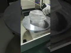
Fused Silica Wafer is made from alumina silicate glass and borosilicate glass. It is an ideal material for many applications due to its excellent optical properties and low coefficient of thermal expansion. It has a wide range of uses including optical components, semiconductor wafers and microelectronic components. Fused Silica Wafer is available in different sizes, ranging from 2 to 12 inch in diameter. It has a bevel of 0.25mm X 45° and has a warp of less than 35um. It has a low TTV of less than 2um and less than 5um. Moreover, it can be coated with AR, HR, and V-Coat for various purposes.
| Material | UV Fused Silica, Fused Quartz (JGS1, JGS2, JGS3) | ||||||
| Specification | unit | 3” | 4” | 5" | 6" | 8" | 12" |
| Diameter (or Square) | mm | 76.2 | 100 | 125 | 150 | 200 | 300 |
| Tol(±) | mm | <0.1~0.25 mm | |||||
| Thinnest Thickness | mm | >0.10 | >0.10 | >0.30 | >0.30 | >0.30 | >0.50 |
| Primary Flat | mm | 22 | 32.5 | 42.5 | 57.5/notch | notch | notch |
| LTV (5mmx5mm) | µm | <2 | <2 | <2 | <2 | <2 | <10 |
| TTV | µm | <8 | <10 | <15 | <20 | <30 | <30 |
| Bow | µm | ±20 | ±25 | ±40 | ±40 | ±60 | ±60 |
| Warp | µm | <30 | <40 | <50 | <50 | <60 | <60 |
| PLTV(<0.5um) | % | ≥95%(5mm*5mm) | |||||
| Transmittance | UV, Optical, IR or Custom option | ||||||
| Edge Rounding | mm | Compliant with SEMI M1.2 Standard/refer to IEC62276 | |||||
| Surface Type | Single Side Polished /Double Sides Polished | ||||||
| Polished side Ra | nm | <1.0nm or specific per requested | |||||
| Back Side Criteria | µm | General is 0.2-0.5µm or as customized | |||||
| Appearance | Contamination | None | |||||
| Particles>0.3µm | <=30 | ||||||
| Saw Marks, striations | None | ||||||
| Scratch | None | ||||||
| Cracks, saw marks, stains | None | ||||||
| Attributes | Values |
|---|---|
| Material | Fused Silica Wafer, High Purity Fused Silica Wafer |
| Refractive Index | 1.46, 1.472, 1.50, 1.51, 1.523 |
| Coating | AR, HR, V-Coat |
| Parallelism | 3 Arc Sec |
| Surface Quality | 20-10 |
| Second Flat | Per Request |
| Application | Semiconductor, MEMS, Medical |
| Transmission | IR, Visible, DUV |
| Schott Model | Borofloat 33, B270, D263, Zerodur, MEMpax, BK7 |
| Metal Impurities | <0.2ppm |
| BOW | <30um |
BonTek's Glass substrates are made from Calcium Silicate Board, borosilicate glass, and Aluminum Silicate Glass and are certified with ISO:9001. Each wafer is packaged in a cassette or jar and can be delivered within 2 weeks after payment is made through TT/in advance. We have a monthly supply ability of 100000 and the wafer is beveled at 0.25mm X 45° with a density of 2.20g/cm3. It also has a coating of AR, HR, or V-Coat and is certified with ISO9001 and RoHS. The damage threshold for BonTek's Fused Silica Wafer is greater than 10J/cm2. Minimum Order Quantity is 5 pcs.
BonTek is a leading supplier of Fused Silica Wafer. We provide custom service based on our customers' needs. Our Fused Silica Wafer can be used for various applications, such as optoelectronic device, light emitting diode, laser diode, etc.
Product Features:
Our Fused Silica Wafer is of high quality, with low OH content, a high refractive index and low warp. We guarantee that all products are strictly tested before delivery.
If you have any inquiries about our Fused Silica Wafer custom service, please don't hesitate to contact us.
Fused Silica Wafer technical support and service is available for customers who need help with their product. Our experienced technical team is available to answer any questions or concerns customers may have. We provide technical support for all our products, including Fused Silica Wafer. We provide comprehensive troubleshooting assistance and will help find solutions to any technical issues.
We also provide product maintenance and repair services. Our team of highly trained technicians can diagnose and repair any Fused Silica Wafer product quickly and efficiently. We have the latest diagnostic tools and can provide fast turnaround times for all repairs.
For customers who need assistance in using Fused Silica Wafer products, we offer comprehensive training services. Our experienced trainers can provide both on-site and remote training to ensure that customers understand how to use their product correctly. We also offer product support documents to help customers with their product.