Add to Cart
LiNbO3 wafers, also known as lithium niobate wafers, are essential components used in a wide range of applications, particularly in the field of photonics and optoelectronics. These wafers are made from high-purity lithium niobate crystals and possess unique crystal structures and exceptional physical properties.
Lithium-Niobate-Wafer (LiNbO3-Substrate) is an ideal substrate material for various optical applications. Our LN-Wafer is made of LiNbO3 material, with 0.5mm thickness, round shape, and surface roughness Ra<0.5nm. The Total Thickness Variation (TTV) can reach as low as 5um, providing highly precise and consistent optical performance. Our Lithium-Niobate-Wafer can be used in various applications such as optical communication, modulators, and optical switches.
| Parameters | Values |
|---|---|
| Material | LiNbO3 |
| Surface Roughness | Ra<0.5nm |
| BOW | <30um |
| Orientation | X-cut |
| Thickness | 0.5mm |
| Warp | <40um |
| Surface | Polished |
| Diameter | 100mm, 150mm, 200mm |
| TTV | <5um |
| Shape | Round Wafer |
BonTek's Lithium-Niobium-Wafer sized from 3 inch to 8 inch. It originates from China and is specially crafted to take the shape of a round wafer with X-Cut Orientation (128Y, 36Y, 64Y, Z cut also available). The thickness of this wafer is 0.5mm and its surface is polished to a smooth finish. The surface roughness of the Lithium Niobate Wafer is Ra<0.5nm, making it ideal for Lithium Niobate Wafer Fabrication.
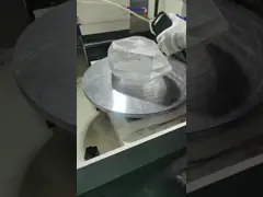
LiNbO3 Wafer Packaging and Shipping
Our LiNbO3 wafers are carefully packed in a sealed and secure container with an anti-static layer and moisture barrier to ensure that it arrives securely and undamaged.
The container is then sealed and labeled with a unique identification number for tracking purposes.
We offer both domestic and international shipping options, with the latter requiring additional paperwork. We also provide a tracking number for all domestic shipments.
For further inquiries about our packaging and shipping services, please contact our customer service team.