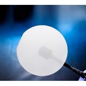
2 Inch 4 Inch 6 Inch Sapphire Single Crystal Wafer With Various Orientations
Brand Name:BonTek
Certification:ISO:9001
Model Number:Sapphire (Al2O3)
Minimum Order Quantity:5 Pieces
Delivery Time:1-4 weeks
Payment Terms:T/T
Contact Now
Add to Cart
Verified Supplier
Location:
Hangzhou Shanghai China
Address:
Room 1106, CIBC, No.198 Wuxing Rd, Hangzhou, P.R.China
Supplier`s last login times:
within 30 hours
Shipping
lt's easy to get a shipping quote! Just click the button below and complete the short form.
Get Shipping Quote
Product Details
Company Profile
Product Details
2 Inch 4 Inch 6 Inch Sapphire Single Crystal Wafer With Various Orientations
Sizes: 2 ", 4 ", 6 "and cut small pieces;
C direction, M direction, R direction; Single side polish, double side polish;
Thickness: 100um, 280um, 300um, 350um, 430um, 500um, 650um, 1mm;
Sapphire is a single crystal of alumina and is the second hardest material in nature, after diamond. Sapphire has good light transmittance, high strength, collision resistance, wear resistance, corrosion resistance and resistance to high temperature and high pressure, biocompatibility, can be made into various shapes of objects. It is an ideal substrate material for making semiconductor optoelectronic devices.
Application: Sapphire single crystal is an excellent multifunctional material. Can be widely used in industry, national defense and scientific research and other fields (such as high temperature resistant infrared window). It is also a widely used single crystal substrate material. Is the current blue, purple, white light emitting diode (LED) and blue laser (LD) industry of the first choice substrate (need to epitaxy gallium nitride film layer on sapphire substrate), is also an important superconducting thin film substrate. In addition to making Y- series, La- series and other high temperature superconducting thin films, it can also be used to grow new practical MgB2 (magnesium diboride) superconducting thin films.
OPTICAL PROPERTIES
Transmission | 0.17 to 5.5 um |
Refractive Index | 1.75449 (o) 1.74663 (e) at 1.06 um |
Reflection Loss | at 1.06 microns (2 surfaces) for o-ray - 11.7%; for e-ray - 14.2% |
Absorption Index | 0.3 x 10⁻³ cm-1 at 2.4 um |
dN/dT | 13.7 x 10⁻⁶ at 5.4 um |
dn/dm = 0 | 1.5 um |
Orientation | R-plane, C-plane, A-plane, M-plane or a specified orientation |
Orientation Tolerance | ± 0.3° |
Diameter | 2 inches, 3 inches, 4 inches, 6 inches, 8 inches or others |
Diameter Tolerance | 0.1mm for 2 inches, 0.2mm for 3 inches, 0.3mm for 4 inches, 0.5mm for 6 inches |
Thickness | 0.25mm, 0.33mm, 0.43mm, 0.65mm, 1mm or others; |
Thickness Tolerance | 25μm |
Primary Flat Length | 16.0±1.0mm for 2 inches, 22.0±1.0mm for 3 inches, 30.0±1.5mm for 4 inches, 47.5/50.0±2.0mm for 6 inches |
Primary Flat Orientation | A-plane (1 1-2 0 ) ± 0.2°; C-plane (0 0-0 1 ) ± 0.2°, Projected C-Axis 45 +/- 2° |
TTV | ≤10µm for 2 inches, ≤15µm for 3 inches, ≤20µm for 4 inches, ≤25µm for 6 inches |
BOW | ≤10µm for 2 inches, ≤15µm for 3 inches, ≤20µm for 4 inches, ≤25µm for 6 inches |
Front Surface | Epi-Polished (Ra< 0.3nm for C-plane, 0.5nm for other orientations) |
Back Surface | Fine ground (Ra=0.6μm~1.4μm) or Epi-polished |
Packaging | Packaged in a class 100 clean room environment |

2 Inch 4 Inch 6 Inch Sapphire Single Crystal Wafer With Various Orientations
Inquiry Cart
0