
Add to Cart
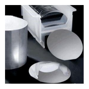
Phi 2'' to 8'' Thermal Oxide Silicon Wafer N-Type P-Type With an Insulating Oxide Layer
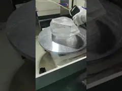
BonTek provides high quality silicon thermal oxide wafers in all diameters from 2″ to 300mm. We ensure your specific requirements are met by choosing prime grade and defecting free silicon wafer as a substrate so that a high uniform layer of thermal oxide is formed in a furnace.
In micro-technology, the main insulating material used is Silicon dioxide which in chemical symbols is written as SiO2. In order to produce an insulating oxide layer, thermal oxidation, which is the most common technique used to obtain the layer is used. The process of obtaining the layer is performed in a furnace.
Thermal Oxide On Both Sides Of Wafer
Film thickness: 100Å – 10µm on both sides
Film thickness Tolerance: Target ±5%
Film stress: - 320±50 MPa Compressive
Film thickness: 100Å – 10,000Å on both sides
Film thickness Tolerance: Target ±5%
Film stress: -320±50 MPa Compressive
SEMI Standard | 2" (50.8mm) | 3" (76.2mm) | 4" (100mm) | 5" (125mm) | 6" (150mm) | 8" (200mm) | 12" (300mm) |
|---|---|---|---|---|---|---|---|
Diameter | 50.8 ± 0.38mm | 76.2 ± 0.63mm | 100 ± 0.5mm | 125 ± 0.5mm | 150 ± 0.2mm | 200 ± 0.2mm | 300 ± 0.2mm |
Thickness | 279 ± 25µm | 381 ± 25µm | 525 ± 20 µm or 625 ± 20µm | 625 ± 20µm | 675 ± 20µm or 625 ± 15µm | 725 ± 20µm | 775 ± 20µm |
Type | P, N or Intrinsic | ||||||
Dopant | B, Ph, As or Undoped | ||||||
Orientation | <100>, <111>, <110> | ||||||
Rsistivity | 0.001 – 300 ohm/cm | ||||||
Primary Flat Length | 15.88 ± 1.65mm | 22.22 ± 3.17mm | 32.5 ± 2.5mm | 42.5 ± 2.5mm | 57.5 ± 2.5mm | Notch | Notch |
Secondary Flat Length | 8 ± 1.65mm | 11.18 ± 1.52mm | 18 ± 2.0mm | 27.5 ± 2.5mm | 37.5 ± 2.5mm | NA | NA |
Surface Finish | SSP, DSP, Etched, or Lapped | ||||||
Acceptance Check
1. The product is fragile. We have adequately packed it and labeled it fragile. We deliver through excellent domestic and international express companies to ensure transportation quality.
2. After receiving the goods, please handle with care and check whether the outer carton is in good condition. Carefully open the outer carton and check whether the packing boxes are in alignment. Take a picture before you take them out.
3. Please open the vacuum package in a clean room when the products are to be applied.
4. If the products are found damaged during courier, please take a picture or record a video immediately. DO NOT take the damaged products out of the packaging box! Contact us immediately and we will solve the problem well.