
Add to Cart
Customizable doping percent LiNbO3 Wafer MgO Er Fe doped Optical grade or SAW grade
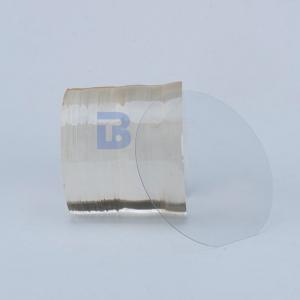
Lithium Niobate (LiNbO3) is a useful optoelectronic material. The material not only has unique piezoelectric, optical and photoelastic properties, but also has good mechanical and chemical stability. Its combination of excellent electro-optic, acoustooptic and nonlinear optical properties makes it an attractive material in integrated optics.
BonTek provides up to 6" diameter, single crystal Optical grade LN material with reduced impurity levels. Other specifications can be provided are doped wafers: Er:LN, MgO:LN and Fe:LN.
The most used SAW orientations are YZ-cut and 128°Y-cut, best fit for television transmission and reception signal processing. The 128°Y-cut with X propagation is said to have the lowest spurious signal level.
Material | 3" 4" 6" 8" LN wafer (Saw/Optical grade) |
Orientation | X / Z / Y41° / Y64° / Y128° / YZ / YX or Customized |
Curie Temp | 1142°C±3°C |
Doped with | Er, MgO, single or double doped available |
Surface finish | single or double sides polish (DLP/SLP/ SSP/DSP all available) |
Thickness | 0.18/0.25/0.35/0.50/1.00 + mm |
TTV | < 1~5µm |
BOW | ± (25µm ~40um ) |
Warp | <= 35µm |
LTV (5mmx5mm) | <1.5 um |
PLTV(<0.5um) | ≥98% (5mm*5mm) with 2mm edge excluded |
Edge | Compl't with SEMI M1.2@with GC800# .regular at C typed |
Orientation flats | available, per request |
Polished side Ra | Roughness Ra<=5A |
Back Side Criteria | Roughness Ra:0.5-1.0µm GC#1000 |
Edge Rounding | Compliant with SEMI M1.2 Standard/refer to IEC62276 |
Cracks, saw marks, stains | None |
Molecular Weight | 147.85 |
Density | 4.65 g/cm³ |
Crystal Class | Rhombohedral |
Moh's Hardness | 5 |
QM | Approx. 10000 |
QE | 1000 |
Melting Temperature | 1253°C |
Curie Point | 1150°C |
Thermal Expansion (@ 25°C) | 15.4 x 10⁻⁶ /°C parallel to C-axis in a temperature range from 0°C
to 110°C. |
Thermal Conductivity (@ 25°C) | 1 x 10⁻² cal/(cm/sec/°C) |
FAQs:
A: We look at ourselves as the piezo wafer specialist. We are the very first to work with Single Crystal Quartz in China about 30 years ago. Then gradually we step in the field of LiNbO3, LiTaO3, Quartz glass, LGS, CTGS etc. Especially, if you are looking for a piezo quartz supplier, we are the ultimate choice! We export millions of quartz blanks each year because we master the AT, SC and IT cuts with superior angle precision.
A: Yes, of course. We can fabricate as per your request. In addition, we are so experienced with piezo wafers that we can provide you relevant suggestions if you are not 100% sure about your choice. Besides, we do have some standard wafers in stock, please check with us.
A: Yes, we would suggest you go with the courier agent you are most familiar with (DHL, FedEX, UPS etc.). We can ship via your account. And, of course, we will pack the products safely in acceptable size to help you save the shipping cost. If you need us to take care of the freight, it’s also not a problem. We also have good discount with the international courier companies.
A: The wafer products are fragile and sometimes expensive. The last thing, as the manufacturer, we want to see is the products we make were damaged during courier. As a result, we will pack the wafers adequately and put them in a proper carton filled with buffer sponge. However, accidents are inevitable sometimes. So, please follow the “Acceptance check” steps shown in the drawings below. If the unwanted happened, we will either give the replenishment or refund if you follow the checking steps.
A: Sure. Factory inspection is important for large quantity purchase and long-term cooperation. Face to face discussion is what we mostly confident with. During the past years, big names around the world have witnessed our progress in factory build-up. These days, due to the Covid-19 pandemic, we also had the experience of videoconferencing with global buyers.
Acceptance Check

