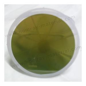
Product Details
4 inch N type SiC ingots and SiC wafers manufacturer
As the leading manufacturer of SiC substrates ,HMT company supply
high quality 4 inch and 6 inch SiC ingots. The average thickness of
SiC ingots are 20mm. We provide conductive N type and
semi-insulating type of SiC ingots. We supply the best price on the
market in worldwide, please feel free to contact us for detailed
specifications. Silicon Carbide is used as substrate for
GaN-epitaxy to produce LEDs in the blue/UV range of the spectrum.
SiC is the material of choice because it offers low lattice
mismatch for III-nitride epitaxial layers and high thermal
conductivity (important for lasers).
Company Profile
Homray Material Technology(HMT)was established in 2009, is a
leading manufacturer and supplier of Silicon Carbide(SiC) Substrate
Wafer, SiC Ingots,SiC Epi Wafer, Gallium Nitride(GaN) Substrate
Wafer(GaN-On-Sapphire Template, Free-standing GaN Wafer), GaN Epi
Wafer (GaN-On-Si Epi Wafer, GaN-On-Sapphire Epi Wafer, GaN-On-SiC
Epi Wafer), and Silicon Test Wafer etc. It is widely acknowledged that compound Semiconductor (GaN, SiC) with its superior
property like wide-bandgap, is expected to the most promising
material choice for next generation device. GaN device/module and
SiC device/module can achieve low losses and fast
switching/oscillation simultaneously because of its high critical
electrical field. Homray Material Technology is committed to
developing high quality GaN Wafer and SiC Wafer for HEMT RF, power
electronics and opto-electronics applications. As the leading
Substrate Wafer and Epi Wafer manufacturer and supplier in the
semiconductor industry, our dealers and partners are mainly
distributed in Europe, USA, Southeast Asia, and South America, our
sales value exceeded 65 Million US dollars in 2020. Excellent products quality and
professional service won the trust and support from our customers
in the world as well as our share of market.