
Add to Cart
Hakko C1390c HDI PCB Vidhan Sabha Exclude From Bom Solidworks Rogers 4003
Welcome to Chengdu Cesgate Technology Co., Ltd
We can provide one-stop service:
PCB circuit boards+Assembly
E-test.
Electronic components purchasing.
PCB assembly: available on SMT, BGA, DIP.
PCBA function test.
Enclosure assembly.
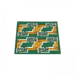
Advantages of HDI PCB
PCB Process - Introduction to HDI
HDI (High Density Interconnect): High-density interconnection
technology, mainly using micro-blind / buried vias (blind / buried
vias), a technology that makes PCB circuit board circuit
distribution density higher. The advantage is that it can greatly
increase the usable area of the PCB circuit board, making the
product as miniaturized as possible. However, due to the increase
in line distribution density, it is impossible to use traditional
drilling methods to drill through holes, and some of the via holes
must be drilled with laser drilling to form blind holes, or
cooperate with inner-layer buried vias to interconnect.
Generally speaking, HDI circuit boards use the build-up method (Build Up), first do or press the inner layers, laser drilling and electroplating on the outer layer are completed, and then the outer layer is covered with an insulating layer (prepreg). ) and copper foil, and then repeat the outer layer circuit making, or continue to laser drill, and stack the layers outward one at a time.
Generally, the diameter of the laser drilling hole is designed to be 3 ~ 4 mil (about 0.076 ~ 0.1 mm), and the insulation thickness between each laser drilling layer is about 3 mil. Due to the use of laser drilling many times, the key to the quality of the HDI circuit board is the hole pattern after laser drilling and whether the hole can be evenly filled after the subsequent electroplating and filling.
Advantages of HDI PCB
1. Can reduce PCB cost. When the PCB density increases beyond eight
layers, it is manufactured by HDI and its cost will be lower than
the traditional complex pressing process.
2. Increase circuit density, interconnection of traditional circuit
boards and parts
3. Promote the use of advanced building techniques
4. Has better electrical performance and signal accuracy
5. Better reliability
6, can improve thermal performance
7. Can improve RFI/EMI/ESD (RFI/EMI/ESD)
8. Improve design efficiency
HDI boards are widely used in mobile phones, digital cameras, MP3,
MP4, notebook computers, automotive electronics and other digital
products, among which mobile phones are the most widely used. HDI
boards are typically fabricated using a build-up method. The longer
the settling time, the higher the technical grade of the board.
Regular HDI boards are basically disposable. High-end HDIs use two
or more build techniques. At the same time, advanced PCB
technologies such as stacked holes, plated hole filling and laser
direct drilling are used. High-end HDI boards are mainly used in 3G
mobile phones, advanced digital cameras, IC carrier boards, etc.
PCB Capacities and Technical Specification
| NO. | Items | Capabilities |
| 1 | Layers | 2-68L |
| 2 | Maximum machining size | 600mm*1200mm |
| 3 | Board thickness | 0.2mm-6.5mm |
| 4 | Copper thickness | 0.5oz-28oz |
| 5 | Min trace/space | 2.0mil/2.0mil |
| 6 | Minimum finished aperture | 0. 10mm |
| 7 | Maximum thickness to diameter ratio | 15:1 |
| 8 | Via treatment | Via, blind&buried via, via in pad, Copper in via … |
| 9 | Surface finish/treatment | HASL/HASL lead free, Chemical tin, Chemical Gold, Immersion gold Inmersion Silver/Gold, Osp, Gold Plating |
| 10 | Base Material | FR408 FR408HR, PCL-370HR;IT180A, Megtron 6(Panasonic);Rogers4350, Rogers4003, RO3003, Rogers/Taconic/Arlon/Nelco laminate with FR-4 material(including partial Ro4350B hybrid laminating with FR-4) |
| 11 | Solder mask color | Green.Black.Red.Yellow.White.Blue.Purple.Matte Green. Matte Black |
| 12 | Testing Service | AOI, X-Ray, Flying-Probe, Function Test, First Article Tester |
| 13 | Profiling Punching | Routing,V-CUT,Beveling |
| 14 | Bow&twist | ≤0.5% |
| 15 | HDI type | 1+n+1,2+n+2,3+n+3 |
| 16 | Min mechanical aperture | 0.1mm |
| 17 | Min laser aperture | 0.075mm |
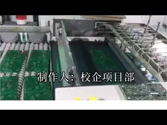
Advanced PCB Manufacturing and PCB Assembly Equipment
CESGATE has imported the advanced machinery from US,Japan,German and Israel to improve our production and technical ability.We have set a great example the PCB field of flying probe testing,buried and blind via and special controlled impedance.We have a highly developed R&D division which has helped our factory successfully produce mechanical micro via,high density impedance and HDI.
FAQ
| Q. What file formats do you accept for production? CESGATE: Gerber file: CAM350 RS274X PCB file: Protel 99SE, P-CAD 2001 PCB BOM: Excel (PDF,word,txt) |
| Q: What is your inspection policy? How do you control the quality? CESGATE: In order to ensure the quality of PCB products, flying probe inspection is usually used; electrical fixtures, automatic optical inspection (AOI), BGA parts x-ray inspection, first article inspection ( FAI) etc. |
| Q: Why choose us? CESGATE: Professional and experienced R&D team. Advanced production equipment, scientific and reasonable process flow. Reliable and strict quality control system. We test all our products before shipment to make sure everything is in perfect condition. |
| Q: WHAT IS YOUR MOQ? CESGATE: MOQ is SPQ normally, while it depends on your specific order. (Sample is available if the buyer can afford the shipping fee.) |
| Q: What does CESGATE need for a customized PCB order? CESGATE: When you place a PCB order, the customers need to provide Gerber or pcb file. If you do not have the file in the correct format, you can send all the details related to the products. |