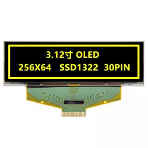
Home /Optoelectronic Displays /

Indoor OLed Display Module, 3.12" 256*64 Dots Oled Display Module, OLed Display Module Controller

Indoor OLed Display Module, 3.12" 256*64 Dots Oled Display Module, OLed Display Module Controller

Brand Name:SAEF
Certification:ISO9001 / ISO14000
Model Number:SFOS312YZ-7091AN
Minimum Order Quantity:3 pcs
Delivery Time:3-5 weeks
Payment Terms:L/C, , T/T, Western Union
Contact Now

Add to Cart

Verified Supplier
Location: Shenzhen China
Address: 3 FL., Yuan Yi Yuan Industrial Park, QianJing Rd, XiXiang, BaoAn,ShenZhen, China
Supplier`s last login times: within 41 hours
Shipping
lt's easy to get a shipping quote! Just click the button below and complete the short form.
Get Shipping Quote
Product Details Company Profile
Product Details

Indoor OLed Display Module, 3.12" 256*64 Dots Oled Display Module, OLed Display Module Controller

Display Description


The Organic Light-Emitting Diode (OLED) is a new generation technology, brighter and clearer images with more agile responding speed. This OLED 3.12" inch model no. SFOS312YZ-7091AN OLED display is made of 256 x 64 dots individual mono color. This OLED module is lightweight, low power and small, there are different interfaces optional; it is default SPI, Parallel and I2C interface.


The size of the active area is 3.12” diagonal with module dimension 88.00 (W) x27.80 (H) mm, active area dimension 76.78 (W) x 19.18 (H) mm. This 3.12 inches OLED display has built-in IC SSD1322 and boasts high contrast ratio 20,000 : 1. Logic supply voltage ranges from 2.4V-2.6V, the typical value is 2.5V. It is great for the application such as medical device, POS system, white goods, home applications, industrial instrument, automation, audio/visual display systems, personal care appliances, household goods, automobile displays, Dynamic information displays etc.


Product:3.12" Inch Passive OLEDResolution:256x64 Pixels Resolution
Display Mode:Passive MatrixInterface:Parallel, SPI Optional
Display Color:White, YellowOptics:All Viewing Angles
Outline Dim.:88.00 (W) X27.80 (H)Active Area:76.78 (W) X 19.18 (H)
Pixel Pitch:0.30 (W) X 0.30 (H)Operating Temp:-40°C To +80°C
Storage Temp.:-40°C To +85°CDriver IC:SSD1322
Supply Voltage:2.4 - 3.5VPin Number:30 Pins
Compliance:REACH & RoHS CompliantIC Package Type:COF
Module Connecting Type:ZIFDuty:1/64

Organic light-emitting diode (OLED), also known as organic laser display and organic electroluminescence display (OLED), refers to the phenomenon that organic semiconductor materials and light-emitting materials are driven by an electric field and emitted through carrier injection and recombination to cause luminescence.
Generally speaking, OLED can be divided into two types according to light-emitting materials: small molecule OLED and polymer OLED (also known as PLED).
OLED is a device that uses a multi-layer organic thin film structure to produce electroluminescence, which is easy to fabricate and requires only a low driving voltage, these main characteristics make OLED very prominent in meeting the application of flat panel displays. OLED displays are thinner and lighter than LCDs, with high brightness, low power consumption, fast response, high definition, good flexibility, and high luminous efficiency, which can meet the new needs of consumers for display technology. More and more display manufacturers around the world have invested in research and development, which has greatly promoted the industrialization process of OLED.


(1) Classification from the device structure
OLED is an organic light-emitting device, which is composed of special organic materials, which can be divided into four types according to its structure, namely single-layer devices, double-layer devices, three-layer devices and multi-layer devices.
1.Single-layer devices
A single-layer device is an organic layer that emits light between the positive and negative electrodes of the device, and its structure is a substrate/ITO/light-emitting layer/cathode. In this structure, due to electrons, hole injection, and unbalanced transmission, the efficiency and brightness of the device are low, and the stability of the device is poor.
2.Double-layer devices
On the basis of the single-layer device, the double-layer device adds a hole transport layer (HTL) or an electron transport layer (ETL) on both sides of the light-emitting layer, which overcomes the problem of carrier injection imbalance of the single-layer device, improves the voltage-current characteristics of the device, and improves the luminous efficiency of the device.
3.Three-layer devices
The three-layer device structure is the most widely used structure, and its structure is substrate/ITO/HTL/light-emitting layer/ETL/cathode. The advantage of this structure is that the exciton is confined to the light-emitting layer, which in turn improves the efficiency of the device.
4. Multi-layer structure
The performance of multi-layer structure is a relatively good structure, which can play a good role at all levels. The light-emitting layer can also be composed of multiple layers, which can be optimized separately because the emitter layers are independent of each other. As a result, this structure can give full play to the role of each organic layer, which greatly improves the flexibility of device design.


(2) Classification from the driving mode
OLED is divided according to the driving mode, which is generally divided into two types, one is active and the other is passive. The active type is generally actively driven, and the passive type is passively driven. In the actual application process, the active driver is mainly used for high-resolution products, while the passive driver is mainly used in the display with a relatively small display size.


(3) Classification from the material
The materials that make up OLED are mainly organic substances, which can be divided according to the types of organic substances, one is small molecule, and the other is polymer. The main difference between these two devices is in the manufacturing process, the small molecule device mainly uses the vacuum thermal evaporation process, and the polymer device uses the rotary coating or spraying printing process.


Structure

OLED devices are composed of substrates, cathodes, anodes, hole injection layers (HIL), electron injection layers (EIL), hole transport layers (HTL), electron transport layers (ETL), electron blocking layers (EBL), hole blocking layers (HBL), and light-emitting layers (EML). Among them, the substrate is the basis of the entire device, and all functional layers need to be evaporated onto the substrate of the device; Glass is usually used as the substrate for the device, but if you want to make a flexible OLED device that can be bent, you need to use other materials such as plastic as the substrate for the device. The anode is connected to the positive pole of the device with the external driving voltage, and the holes in the anode will move to the light-emitting layer in the device under the drive of the external driving voltage. The most commonly used material for anodes is ITO. The hole injection layer can modify the anode of the device, and can make the hole from the anode smoothly injected into the hole transport layer. The hole transport layer is responsible for transporting the holes to the light-emitting layer; The electron barrier layer will block the electrons from the cathode at the light-emitting layer interface of the device, increasing the concentration of electrons at the light-emitting layer interface of the device. The light-emitting layer is where the electrons and holes of the device are recombined to form excitons, and then the excitons deexcite the light; The hole barrier layer will block the holes from the anode at the interface of the light-emitting layer of the device, thereby increasing the probability of recombination of electrons and holes at the interface of the light-emitting layer of the device, and increasing the luminous efficiency of the device. The electron transport layer is responsible for transporting electrons from the cathode into the light-emitting layer of the device; The electron injection layer plays the role of cathodic modification and electron transport to the electron transport layer; The electrons in the cathode move towards the light-emitting layer of the device driven by the applied driving voltage applied to the device, and then recombine with the holes from the anode in the light-emitting layer.


Luminescence principle

The luminescence process of OLED devices can be divided into: electron and hole injection, electron and hole transport, electron and hole recombination, and exciton deexcitation. Specifically:
(1) Injection of electrons and holes. In the process of moving to the light-emitting layer of the device, if the device contains an electron injection layer and a hole injection layer, the electrons and holes first need to overcome the energy level barrier between the cathode and the electron injection layer and between the anode and the hole injection layer, and then move to the electron transport layer and the hole transport layer of the device through the electron injection layer and the hole injection layer. Electron injection layers and hole injection layers increase the efficiency and lifetime of the device. The mechanism of electron injection in OLED devices is still being studied, and the most commonly used mechanisms are tunneling and interfacial dipole mechanisms.
(2) Electron and hole transport. Driven by the applied driving voltage, the electrons from the cathode and the holes of the anode will move to the electron transport layer and hole transport layer of the device, respectively, and the electron transport layer and hole transport layer will move the electrons and holes to the interface of the light-emitting layer of the device, respectively. At the same time, the electron transport layer and the hole transport layer block the holes from the anode and the electrons from the cathode at the interface of the device's light-emitting layer, respectively, so that the electrons and holes at the interface of the device's light-emitting layer can accumulate.
(3) Recombination of electrons and holes. When a certain number of electrons and holes at the interface of the device's light-emitting layer reaches a certain number, the electrons and holes are recombined to generate excitons in the light-emitting layer.
(4) De-excitation of excitons. The excitons generated at the light-emitting layer will activate the organic molecules in the light-emitting layer of the device, and then make the outermost electrons of the organic molecules transition from the ground state to the excited state.


Display technology


classify
1. OLED display technology is divided into two categories according to the manufacturing method: polymer process and small molecule process, polymer process (PLED) does not require thin film process, so the equipment investment and production cost are much lower than TFT-LCD (similar to CD-R in the form of spin-coating by rotary coating), which is more conducive to the development of large-size displays. However, due to the different attenuation constants of each color of PLED, it is not only difficult to diversify the product, but also affects the service life of the product. Although small molecule organic excitation optical elements are better than polymer organic organic excitation optical elements in terms of colorization, the equipment investment and production cost are high (due to the evaporation of multi-layer organic thin film materials by heating and evaporation method, in order to avoid mutual contamination between materials, expensive multi-cavity vacuum equipment must be used, and the driving voltage is large and the output rate is low).
Polymer components have better thermal stability, so they can be suitable for higher temperature operating environments and can tolerate higher current densities, but due to the difficulty of independent positioning of red basket and green three-color pixels, it is still impossible to launch full-color displays.
2. OLED display technology is divided into two categories: passive (passive drive passive matrix, i.e., PM-OLED) and active (active drive active matrix, i.e., AM-OLED) according to the driving mode. The passive type is suitable for small format because its instantaneous brightness is proportional to the number of cathode scanning columns, so it needs to be operated at high pulse current, which will shorten the lifetime of the pixels. And because of the scanning, its resolution is also limited, but the low cost and simple process are its major advantages.
Although the cost is more expensive and the process is more complex (still easier than TFT-LCD), each pixel can be driven continuously and independently, and the drive signal can be memorized, without the need to operate under high pulse current, with high efficiency and extended life, which is suitable for full-color OLED display products with large size and high resolution and high information capacity.


advantage
1. Compared with the crystal layer of LED or LCD, the organic plastic layer of OLED is thinner, lighter and more flexible.
2. The light-emitting layer of OLED is relatively light, so its base layer can use flexible materials instead of rigid materials. The OLED base layer is made of plastic, while the LED and LCD base layer is made of glass.
3. OLED is brighter than LED, and the organic layer of OLED is much thinner than the corresponding inorganic crystal layer in LED, so the conductive layer and emission layer of OLED can adopt a multi-layer structure. In addition, LEDs and LCDs require glass as a support, and glass absorbs a portion of the light. OLEDs do not require the use of glass.
4. OLED does not need to use the backlight system in LCD. LCD works selectively blocking certain backlit areas to make the image visible, while OLED emits light on its own. Because OLEDs do not require a backlit system, they consume less power than LCDs (most of the power consumed by LCDs is used in backlit systems). This is especially important for battery-powered devices, such as mobile phones.
5. OLED is easier to manufacture and can also be made into larger sizes. OLED is made of plastic, so it can be made into a large area of thin sheets. It is much more difficult to use so many crystals and lay them out.
6. OLED has a wide field of view, up to about 170 degrees. However, LCD has to block light when it works, so there are natural obstacles to observation at certain angles. OLED itself can emit light, so the field of view is also much wider.


characteristic

OLED technology can be widely used because it has the following advantages compared with other technologies:
(1) Low power consumption
Compared with LCD, OLED does not need a backlight, and the backlight is a more energy-consuming part of LCD, so OLED is more energy-efficient. For example, a 24-inch AMOLED module consumes only 440 MW, while a 24-inch polysilicon LCD module reaches 605 MW.
(2) Fast response
Compared with other technologies, OLED technology has a fast response time, which can reach the microsecond level. The higher response speed makes it better to achieve moving images. According to the relevant data analysis, its response speed has reached about 1000 times the response speed of the liquid crystal display.
(3) Wider viewing angle
Compared with other displays, OLED is actively emitting light, so the picture will not be distorted in a wide range of viewing angles. The width of the viewing angle is more than 170 degrees.
(4) It can achieve high-resolution display
Most high-resolution OLED displays use active matrix, that is, AMOLED, and its light-emitting layer can absorb 260,000 true colors with high resolution, and with the development of science and technology, its resolution will be higher in the future.
(5) Wide temperature characteristics
Compared with LCD, OLED can work in a wide range of temperatures, and according to relevant technical analysis, the temperature can operate normally from -40 degrees Celsius to 80 degrees Celsius. This allows for lower geographical restrictions and can be used normally in extremely cold regions.
(6) OLED can achieve a soft screen
OLED can be produced on different flexible substrate materials such as plastics and resins, and the organic layer can be evaporated or coated on a plastic substrate to achieve a soft screen.
(7) The quality of OLED finished products is relatively light
Compared with other products, the quality of OLED is relatively small, the thickness is relatively small compared with LCD, and its seismic coefficient is higher, which can adapt to large acceleration, vibration and other harsh environments.


Lifespan influencing factors

There are many factors that affect the life of OLED devices, and according to the factors affecting OLED devices, the influencing factors can be divided into two types: internal and external. Among them, the internal factor refers to the decrease in the life of the device is caused by non-external factors such as the material or structure of the device itself, and the external factor refers to the decrease in the life of the device is caused by the external factors of the environment in which the device is located.
The external factors that affect the life of OLED devices include the content of water, oxygen, and tiny particles in the environment where the device is located, the flatness of the substrate surface, and the tiny pores on the electrode surface of the device. When it meets with water and oxygen in the environment, the electrodes in the device are very easy to react with water and oxygen, and produce black dots that cannot emit light in the light-emitting area of the device, and the size of the black dots will gradually increase with time, so that the area of the light-emitting area of the device will gradually decrease. The tiny particles in the environment in which an OLED device is exposed can also have a significant impact on the lifetime of the device. In the process of preparing OLED devices, if the substrate of the device is not cleaned when cleaning, or if there are many tiny particles in the evaporation environment of the device during the evaporation process, the tiny particles remaining on the substrate will have an important impact on the life of the device. When attached to the electrode surface of the device, the tiny particles will reduce the conductivity of the electrode where it is located, and affect the flatness of the functional layer on the electrode surface of the electrode, which in turn affects the life of the device. The flatness of the surface of the device substrate also affects the lifetime of the OLED device. If the surface of the device substrate is uneven and there are many protrusions, the protrusions generated are easy to cause tip discharge, which in turn causes the device to generate more leakage current. In addition, tip discharge will also cause more heat generated by the device, which in turn will affect the stability of the device and reduce the lifetime of the device. The tiny pores on the surface of the electrodes of the device can also affect the lifetime of the OLED device. The reason is that if there are more pores on the electrode surface of the device, the water and oxygen in the environment where the device is located are more likely to enter the inside of the device through the pores on the electrode surface and react with the materials in the device, which will affect the stability of the device and reduce the life of the device.


The internal factors that affect the life of OLED devices include the structure of the device and the stability of the materials used in the device. Generally speaking, OLED devices with multilayer structure have a longer life span than OLED devices with single-layer structure; Compared with single-layer devices, multi-layer devices require a lower driving voltage to be injected into the device due to the smaller energy level barriers that electrons and holes need to overcome when they are injected into the cathode and anode. In addition, the luminous efficiency of multilayer devices will be higher due to the addition of functional layers such as electronic barrier layer, hole barrier layer, electron transport layer and hole transport layer. The stability of the materials used in the device will also affect the life of the OLED device; Since the device generates more heat when driven by an applied driving voltage, the lifetime of the device will also be reduced if the stability of the materials used in the device is poor.


Fields of application


Due to the many advantages of OLED, OLED technology is more widely used than LCD technology, which can be extended to the field of electronic products, commerce, transportation, industrial control, and medical fields.
In the commercial field, POS machines, copiers, and ATMs can be installed with small-sized OLED screens, which are both beautiful and practical due to their bendable, thin, and anti-aging properties. The large screen can be used as a business promotion screen, and can also be used as an advertising screen for stations, airports, etc., because the OLED screen has a wide viewing angle, high brightness, bright colors, and a much better visual effect than the LCD screen.
In the field of electronic products, OLED is the most widely used in smart phones, followed by notebooks, displays, TVs, tablets, digital cameras and other fields, because the OLED display color is more intense, and the color can be adjusted (different display modes), so it is very widely used in practical applications, especially today's curved TV, widely praised by the masses.
It is necessary to mention a little VR technology here, LCD screen viewing VR equipment has a very serious drag, but it will be relieved a lot in OLED screen, this is because OLED screen is to light up light molecules, and liquid crystal is light liquid flow. Therefore, in 16 years, the OLED screen officially surpassed the LCD screen and became the new darling of the mobile phone industry.
In the field of transportation, OLED is mainly used as ships, aircraft instruments, GPS, video phones, vehicle displays, etc., and mainly in small size, these fields mainly focus on OLED wide viewing angle performance, even if you do not look directly can clearly see the screen content, LCD is not.

In the industrial field, today's China's industry is developing in the direction of automation and intelligence, and more and more intelligent operating systems have been introduced, which has more demand for screens. Whether it is on a touch screen display or a viewing display, OLED has a wider range of applications than LCD.
In the medical field, the impact of medical diagnosis and surgical screen monitoring are inseparable from the screen, in order to meet the requirements of the wide field of view of medical display, OLED screen is the "best choice".
It can be seen that the development space of OLED display is very high, and the market potential is huge. However, compared with LCD screens, OLED manufacturing technology is not mature enough, due to the low mass production rate and high cost, only some high-end devices in the market will use top-of-the-line OLED screens. However, judging from the data in the first half of 2017, various manufacturers have increased their investment in OLED technology, and many mid-range electronic products in China have applied OLED displays. From the perspective of the mobile phone industry, since 2015, the proportion of OLED screen applications has increased year by year, although there are still no LCD products, but high-end smartphones have adopted the most advanced OLED screens, therefore, the development of electronic products such as smart phones, is bound to further promote the development of OLED.


Trends

1. It can really give full play to the advantages of OLED technology, and it is still dominated by AMOLED applications
In terms of the structure and composition of its components, PMOLED is simpler than AMOLED, has the manufacturing advantage of mass production and low cost, and is also the earliest mass production product form of OLED for display applications. PMOLED is suitable for mobile phone display screen applications, especially in small panel applications with low message display, and the mass production cost is relatively low. However, when the main application products are increasingly turning to the application direction of high-color, large-size, and fast display, PMOLED is obviously unable to meet the new needs in terms of technical conditions. However, the real advantages of OLED technology are still mainly used in AMOLED applications, especially in display applications.
2. Flexible AMOLED can be applied
For example, Sony has developed a flexible plastic substrate with an AMOLED structure, which is made by applying the AMOLED structure to a plastic film, overcoming the deformation of the plastic substrate that may be caused by the high-temperature manufacturing process of AMOLED. In Sony's manufacturing method, the flexible OLED panel manufacturing process can be controlled below 180°C throughout the process.
Prototype development for flexible OLEDs, Arizona State University (Arizona State University; ASU) has also developed a 4-inch AMOLED display, which is now available in QVGA display resolution. The flexible design prototype developed by ASU uses DuPont Teijin thermally stabilized polyethylene naphthalate ethylene glycol (PEN) material, which is manufactured in the same sub-180°C process as Sony, and integrated into an amorphous silicon TFT backplane.

3. The development of energy-saving light source OLED has become a global trend
The material characteristics of OLED not only amaze display manufacturers, but also the self-luminous characteristics of OLED also interest lamp and light source manufacturers, such as Philipss, Osram and other major lighting manufacturers to try to invest in related research and development.
In 2022, the first fully 3D printed flexible OLED display was launched.
In December 2022, according to Videotelen News, LG Display's focus in 2023 is the OLED product line, and a number of high-end OLED e-sports products are planned to be launched in the first half of the year, covering the size from 27 inches to 45 inches.
On April 27, 2023, the Korea Display Industry Association released the main statistics of the global display industry in 2022. According to the statistics, South Korea maintains a relatively leading position in the field of organic light-emitting diode (OLED) displays, with a market share of 81.3%.
In May 2023, at the annual Display Week trade show in Los Angeles, Samsung showcased a revolutionary 12.4-inch rollable OLED panel.


3.12" Inch 256x64 Pixels Resolution COF OLED display with SSD1322 Parallel SPI IInterface Drawing


3.12" Inch 256x64 Pixels Resolution COF OLED display with SSD1322 Parallel SPI IInterface Product Image


CONTACT


Welcome to inquire via ck@saef.com.cn


Search Keyword: 256x64 oled, oled 256x64, 3.12" oled, 3.12 inch oled, oled 3.12", SPI OLED display 3.12 inch, SPI OLED display 3.12", SSD1322 OLED Display, SSD1322 OLED 3.12", micro OLED 3.12 inch, 3.12 inch mini OLED display, 3.12 inch thin OLED display, 3.12" tiny OLED display, 3.12 inch white OLED display, OLED touch display 3.12 inch.


China Indoor OLed Display Module, 3.12 256*64 Dots Oled Display Module, OLed Display Module Controller supplier

Indoor OLed Display Module, 3.12" 256*64 Dots Oled Display Module, OLed Display Module Controller

Inquiry Cart 0