Mobile Phone 5G Electronics PCB PCBA Motherboard HASL OSP
Brand Name:IBE
Certification:ISO/TS16949 ISO13485
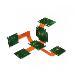
Model Number:Flex Rigid PCB
Minimum Order Quantity:10
Delivery Time:5-8 working days
Payment Terms:D/A, L/C, D/A, D/P, T/T, Western Union, MoneyGram
Contact Now
Add to Cart
Verified Supplier
Supplier`s last login times:
within 39 hours
Product Details
Company Profile
Product Details
OEM ODM Multilayer Mobile Phone PCB 5g Electronic Rigid-Flex Printed Circuit Board PCBA Motherboard
About IBE Corporation
Founded in 2005, IBE Corporation is a mid-size provider of
end-to-end electronics manufacturing services (EMS) including PCBA
production, systems integration and comprehensive testing services,
enclosure fabrication, as well as product design, sustaining
engineering and supply chain management services. IBE facilities
span a broad footprint in the China,United States and Vietnam. IBE
services extend over the entire electronic product life cycle from
the development and introduction of new products through to the
growth, maturity and end-of-life phases.
PCBA Capability
The main SMT production line consists of automated high-precision
state-of-the-art equipments from PanasonIC,Sumsung, Japan total 6
lines (Smallest SMT components size can reach to 0201,capable of
0.6mm*0.3mm ~ 50mm*50mmQFP, 0.15mm gap, ±0.05 accuracy ),
EMS capacity can reach 150,000,000 components per month.
Our engineering team has extensive experience in DFM/DFA/DFT
technologies.
SMT, BGA Rework, Re-balling, X-Ray are all readily achieveable.
Stencils can
be cut and delivered inside of 4 hours.
| 1 | Material | PR4,Halogen free, High TG,CEM3,PTFE,Aluminum BT,Rogers |
| 2 | Board Thickness | Mass Production:0.3-3.5mm Samples:0.21-6.0mm |
| 3 | Surface Finish | HASL,OSP,Immersion Silver/Gold/SN,Flash Gold, Gold Finger,Hard Gold Plating |
| 4 | PCB Panel Size | Max Mass Productoin: 610x460mm Sample:762x508mm |
| 5 | Layer | Mass production:2-58 Layers, Samples:1-64 Layers |
| 6 | Min. Drill Hole Size | Laser Drill 0.1mm,Machine Drill 0.2mm |
| 7 | PCBA QC | X-ray,AOI Test,Functional Test |
| 8 | Speciality | Automotive,Medical/Gaming/Smart Device,Computer,LED/Lighting,etc |
| 9 | Sanforized | Buried via, Blind via, Mixed Pressure,Embedded Resistance,Embedded Capacitance, Local Mixed Pressure, Local High Density, Back Drill, Impedance Control |
Delivery Time:
Order Conditions | Standard Delivery Date | The fastest Delivery Date |
Prototype ( <20pcs) | 2days | 8hours |
Small Volume (20-100pcs) | 6days | 12hours |
Medium Volume (100-1000) | 3days | 24hours |
Mass Production (>1000) | Depends on BOM | Depends on BOM |
FAQ:
1.How does a printed circuit board assembly (PCB assembly) work?
The primary function of a PCB assembly is to integrate the
electronic components of a device into a compact or defined space.
Acting as the central hub of the electronic circuit of a device,
the PCB provides insulation for all other electrical components,
allowing them to be safely connected to a power source.
2. What information is required for a turnkey PCB assembly order?
For turnkey projects, we’ll need the following:
Gerber file
Bill of materials (BOM)
Component placement list (CPL)
All relevant CAD and .stp file
3. Are you UL / Underwriters Laboratory approved?
IBE pursues all applicable UL certifications for our products, and
we offer several products certified with UL and CSA based on
customer’s demand
Underwriters Laboratories (UL) grants multiple certifications,
including:
IBE is certified for PCB by UL file E326838


Mobile Phone 5G Electronics PCB PCBA Motherboard HASL OSP
Inquiry Cart
0