Remote Key Fob 2 Layer PCB FR4 1.0 MM Thickness 35 UM Copper
Brand Name:WITGAIN PCB
Certification:UL
Model Number:PCB000031
Minimum Order Quantity:1 pcs/lot
Delivery Time:10 days
Payment Terms:T/T
Contact Now
Add to Cart
Active Member
Location:
Shenzhen China
Address:
Room 1520, Block 11, International E-Commerce Logistics Center, PingAn Road, PingHu Street, LongGang District, ShenZhen City, China 518111
Supplier`s last login times:
within 1 hours
Product Details
Company Profile
Product Details
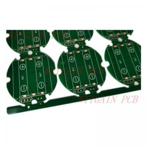
2 Layer FR4 Printed Circuit Board 1.0 MM Thickness Used In Remote Key
- Main Features:
1 2 Layer FR4 substrate material printed circuit board.
2 Double layer copper, copper thickness is 35um/35um.
3 Finished pcb thickness is 1.2mm.
4 PCB drawing size is 128.82mm*96.14mm/6pcs
5 Immersion Gold treatment
6 2 layer pcb with 6/6mil min line space and width.
7 Green solder mask and white silkscreen.
8 Need customer to send us the gerber file or PCB file
- Our Capabilities:
| NO | Item | Capability |
| 1 | Layer Count | 1-24 Layers |
| 2 | Board Thickness | 0.1mm-6.0mm |
| 3 | Finished Board Max Size | 700mm*800mm |
| 4 | Finished Board Thickness Tolerance | +/-10% +/-0.1(<1.0mm) |
| 5 | Warp | <0.7% |
| 6 | Major CCL Brand | KB/NanYa/ITEQ/ShengYi/Rogers Etc |
| 7 | Material Type | FR4,CEM-1,CEM-3,Aluminum,Copper, Ceramic, PI, PET |
| 8 | Drill Hole Diameter | 0.1mm-6.5mm |
| 9 | Out Layer Copper Thickness | 1/2OZ-8OZ |
| 10 | Inner Layer Copper Thickness | 1/3OZ-6OZ |
| 11 | Aspect Ratio | 10:1 |
| 12 | PTH Hole Tolerance | +/-3mil |
| 13 | NPTH Hole Tolerance | +/-1mil |
| 14 | Copper Thickness of PTH Wall | >10mil(25um) |
| 15 | Line Width And Space | 2/2mil |
| 16 | Min Solder Mask Bridge | 2.5mil |
| 17 | Solder Mask Alignment Tolerance | +/-2mil |
| 18 | Dimension Tolerance | +/-4mil |
| 19 | Max Gold Thickness | 200u'(0.2mil) |
| 20 | Thermal Shock | 288℃, 10s, 3 times |
| 21 | Impedance Control | +/-10% |
| 22 | Test Capability | PAD Size min 0.1mm |
| 23 | Min BGA | 7mil |
| 24 | Surface Treatment | OSP, ENIG,HASL, Plating Gold, Carbon Oil,Peelable Mask etc |
- FQA:
Q1: What is Flying Probe Testing?
A1: Flying Probe Testing (FPT) is a automated test used evaluate proper operation of components on a PCB board. In this test two or more probes are programmed to move across the board in the air and access various component pins one by one to detect faults like Opens, Shorts, Resistance values, Capacitance values, and Component Orientation.
These probes have high precision needles which are programmed to fly over the board and test various pins on the board.
Flying Probe Testing is usually used for prototype, low volume and small batch PCB testing. However, the process has also started to be used for high volume testing. In these cases the PCB board travels to the tester though a conveyor belt where the flying probes are programmed to test various pins on the board. The flying probes need to be programmed for each PCB board type.
Features of Flying Probe Testing:
- FPT has fast checking speed and precision since it is software-based.
- The probe can be moved easily from one node to another to provides better precision and accuracy for copper pad placement and solder joints.
- Suitable for small volume production testing
- Tests each component individually and can test LEDs as well
- It doesn’t require test points as it uses vias embedded on the board as the test points.
- A flying probe tester is equipped with a camera to identify missing components and to check the component polarity.
- It is Cost-effective and can test both sides of the board
- Since FPT is software supported, it is easier for the design engineers to take feedback in the case of any error.
- Better access to nodes through vias, leads and SMT lands
This type of testing is called In-Circuit Testing. Another type of In-Circuit Testing is Grid Testing or Bed of Nails Testing.


Remote Key Fob 2 Layer PCB FR4 1.0 MM Thickness 35 UM Copper
Inquiry Cart
0