
Add to Cart
Ps2 Interface Integrated IC Wireless Mouse Chip ROHS Certificate
Wired Wireless Mouse Chip USB Interface Integrated IC Optical Mouse
Chip
Chip name: Optical mouse chip
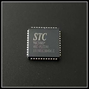
Mouse chip model: GZ-P001-STC
Function description
Timer/counter
The keyboard chip provides three 16-bit timer/counters T0, T1, T2.
Each can be used as a general counter. When T0/T1/T2 is used as a
timer, the time unit used to trigger the timer is the machine
cycle. A machine cycle is equal to 12 or 6 oscillation cycles,
depending on whether the user configures the chip to be in 12T mode
or 6T mode. When T0/T1/T2 is used as a counter, the counting event
is the corresponding pin of T0/T1/T2 High to low level change". In
this mode, the chip samples the T0/T1/T2 pins every machine cycle.
Once the result is from 1 to 0, the chip counts 1 to the counter.
It should be noted that when operating as a counter, the width of
the high pulse or low pulse of the T0/T1/T2 pin must be greater
than one machine cycle. There are two special registers to
configure T0 and T1. They are TMOD, TCON have two special registers
to configure T2. They are T2MOD, T2CON
Serial port (UART)
The serial port of the mouse chip is duplex, it can send and
receive data at the same time. The data sent and received share the
same special register SBUF. There are actually two SBUF registers
inside the chip, one for sending and one for receiving. The serial
port can work in 4 different modes.
Mode 0
Usually, this mode is purely used to expand the I/O port of the
chip. In this mode, both receiving and sending data pass through
the RXD pin, and TXD outputs a synchronous shift clock. What is
sent or received is 8-bit data, with the lowest bit first, and its
baud rate is fixed at 1/12 of the MCU clock.
Mode 1
Send through TXD pin or receive 10-bit data frame through RXD pin.
The data frame includes 1 start bit (0), 8 data bits, and 1 stop
bit (1). After the reception is complete, the stop bit is stored in
RB8 of SCON. Baud rate (mode 1) = 2SMOD X (T1 overflow rate) /32 or
= T2 overflow rate /16
Mode 2
Send through TXD pin or receive 11-bit data frame on RXD pin. The
data frame includes 1 start bit (0), 8 data bits, 1 programmable
9th bit and 1 stop bit (1). When sending, the 9th bit comes from
TB8 of SCON. When receiving, the 9th digit will be stored in TB8 of
SCON. The baud rate can be 1/32 or 1/64 of the clock frequency;
baud rate (mode 2) = 2SMOD X OSC/64
Mode 3
Mode 3 is the same except that the baud rate is different from Mode
2. Baud rate (mode 3) = 2SMOD X (T1 overflow rate) /32 or = T2
overflow rate /16 For all modes, writing to SBUF will start
sending. For mode 0, if RI=0 and REN=1, the reception starts. For
other modes, if REN=1 and a start bit is introduced, that is, if
there is a falling edge, the reception starts.
Power down mode
The user sets PCON.1 to make the chip enter the power-down mode. In
power-down mode, the chip clock is stopped. The internal RAM and
SFR of the chip remain unchanged. The wake-up method can be
hardware reset or /INT0, /ITN1, /INT2 and /INT3 external
interrupts. When the hardware is reset, pay attention to at least
keep the RESET pin high for more than 10ms to stabilize the clock.
The program starts to execute from address 0x0000. If it is an
external interrupt wake-up, the program will jump into the
interrupt vector and perform interrupt processing. In order to use
an external interrupt to wake up, the external interrupt must be
set correctly before entering the power-down mode.
Pin status in IDLE mode and power-down mode:
| Mode | Program space | ALE | PSEN | P0 | P1 | P2 | P3 |
| IDLE | internal | 1 | 1 | Data | Data | Data | Data |
| IDLE | external | 1 | 1 | Float | Data | Address | Data |
| Power down mode | internal | 0 | 0 | Data | Data | Data | Data |
| Power down mode | external | 0 | 0 | Float | Data | Data | Data |
Working voltage | 4.5V~5.5V |
Interface type | USB PS2 |
Lens ratio | 1:1 |
DPI | 800/1200 (default) |
Current (mobile) | 20mA |
Current (not moving) | 5mA |
Current (power down) | 0.5Ma |
Package | DIP12 |
Product image presentation: