
Add to Cart
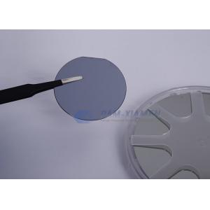
Undoped Germanium Wafer With EPD, 2”-Powerway Wafer
PAM-XIAMEN offers Germanium wafer Single Crystals and Wafers grown by VGF / LEC, we have a strong advantage in providing Ge wafer for micro-electronics and opto-electronics industry in diameter range from 2 inch to 6 inch. Germanium wafer is an elemental and popular semiconductor material, due to its excellent crystallographic properties and unique electric properties, Germanium wafer is widely used in Sensor, Solar cell and Infrared optics applications. PAM-XIAMEN can provide low dislocation and epi ready Germanium wafers to meet your unique germanium requirement.
General Properties Of Germanium Wafer
| General Properties Structure | Cubic, a = 5.6754 Å | ||
| Density: 5.765 g/cm3 | |||
| Melting Point: 937.4 oC | |||
| Thermal Conductivity: 640 | |||
| Crystal Growth Technology | Czochralski | ||
| Doping available | Undoped | Sb Doping | Doping In or Ga |
| Conductive Type | / | N | P |
| Resistivity, ohm.cm | >35 | < 0.05 | 0.05 – 0.1 |
| EPD | < 5×10³/cm2 | < 5×10³/cm2 | < 5×10³/cm2 |
| < 5×10²/cm2 | < 5×10²/cm2 | < 5×10²/cm2 | |
Specification of Germanium Wafer
| Item | Specifications | Remarks |
| Growth Method | VGF | |
| Conduction Type | undoped | |
| Dopant | NONE | |
| Wafer Diamter | 2 | inch |
| Crystal Orientation | (100),(111),(110) | |
| Thickness | 200~550 | um |
| OF | EJ or US | |
| Carrier Concentration | request upon customers | |
| Resistivity at RT | (0.001~80) | Ohm.cm |
| Etch Pit Density | <5000 | /cm2 |
| Laser Marking | upon request | |
| Surface Finish | P/E or P/P | |
| Epi ready | Yes | |
| Package | Single wafer container or cassette |
Germanium Wafer Process
In the germanium wafer production process, germanium dioxide from the residue processing is further purified in chlorination and hydrolysis steps.
1) High purity germanium is obtained during zone refining.
2) A germanium crystal is produced via the Czochralski process.
3) The germanium wafer is manufactured via several cutting, grinding, and etching steps.
4) The wafers are cleaned and inspection. During this process, the wafers are single side polished or double side polished according to custom requirement, epi-ready wafer comes.
5) The wafers are packed in single wafer containers, under a nitrogen atmosphere.
Application:
Germanium blank or window are used in night vision and thermographic imaging solutions for commercial security, fire fighting and industrial monitoring equipment. Also, they are used as filters for analytical and measuring equipment, windows for remote temperature measurement, and mirrors for lasers.
Thin Germanium substrates are used in III-V triple-junction solar cells and for power Concentrated PV (CPV) systems
PAM-XIAMEN offer germanium wafers. No matter what the project or use is, we have germanium wafers available at competitive prices. Enquire us today to learn more about how we can help you with all your wafer needs.

