Add to Cart
Electronics PCB Material FR4 1.5mm 35/35um Copper Immersion Tin Green Soldermask
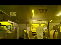
Linked Electronics is specialists in the high quality, advanced technology solutions for both PCB fabrication and SMT assembly with flexible delivery capabilities
Shenzhen OEM PCB Assembly Manufacturing
Linked Electronics is Electronic PCB & PCBA manufacturer
Specifications:
1.Fast and one-stop service
2.Accept PCB design,clone and OEM/ODM service.
3.PCB+Components+PCBA
4.Quote within 48 hours for PCBA projects and 2 hours for PCB fabrication projects
Contact us today and let's discuss about your PCB demand today.
PCB Capabilities
| Standard | IPC Class2/IPC Class3 | √ |
| Products& Manufacture | Available laminate | FR-4 High TG material Halogen free FR-4 FR-1,CEM-1, Aluminum base |
| PCB Maximum Layer | 64 | |
| Board Thickness | 0.2mm to 7mm | |
| Min. Track Width/Space | 2mils/2mils | |
| Min. Annular Ring | 3mils | |
| Min. finished hole size | 4mils/0.1mm | |
| Copper thickness | 0.5oz to 20oz | |
| Impedance control | +/-10% | |
| Surface Finishing | Lead Solder HASL | √ |
| Lead-Free Solder LF HASL | √ | |
| Immersion Gold/ENIG | √ | |
| Immersion Silver | √ | |
| Immersion Tin | √ | |
| OSP | √ | |
| Carbon Priting | √ | |
| Gold finger | √ | |
| Outline Profiling | CNC Routing | √ |
| V-Groove | √ | |
| Punching | √ | |
| Edge Plating | √ | |
| File Format | GERBER | √ |
| PROTEL 99SE | √ | |
| PROTEL DXP | √ | |
| POWER PCB | √ | |
| CAM350 | √ | |
| GCCAM | √ | |
| ODB+(.TGZ) | √ |
Following Techniques on the PCB boards is within our capabilities at Linked Electronics, the PCB manufacture in China.
PCB Process
Immersion Tin PCB Board
The Immersion Tin surface treatment on the PCB boards has a very thin layer of tin, applied over the copper layer on the electronic PCB. This method is a Lead-Free PCB alternative but has a consistently flat surface, which solders well but the cost is relatively higher than HASL Lead Free. This tin surface finish can protect the copper under the tin layer from oxidation for 1 year according to IPC standard.
The Immersion Tin surface finish has a relatively long shelf life
compared to other surface treatment , but does require careful
handling during the PCB Assembly Process. Copper and tin however have a strong affinity for one another.
The diffusion of one metal into the other will occur inevitably,
directly impacting the shelf life of the deposit and the
performance of the finish. The negative effects of tin whiskers
growth are well described in industry related literature and topics
of several published papers.
Pros
| Cons
|
If you have any more questions regarding the immersion Tin PCB boards, contact us today, our sales team and engineering team will be very pleased to answer your questions, look forward to seeing you soon.
Quality Assurance at Linked Electronics for PCB Manufacturing:
Preventive control through engineering design before production.
Quality management system and products are certified by
authoritative organizations.
Consistant production process control all the time for all types of
PCBs.
Perfect product quality improvement system.
100% inspection including e-testing and AOI inspection.
High voltage testing, impedance testing, micro-sections, solderability testing, and other professional tests are available.
All electronics PCBs boards are packed in a vacuum package and then put into a solid carton box, which will ensure no damages happen during the shipment. Should there is any damages, contact us for the losses.