Blind Buried Holes FR4 EM370 8 Layer HDI PCB Board
Brand Name:WITGAIN PCB
Certification:UL Certificate
Model Number:S08E4651A0
Minimum Order Quantity:Negotiable
Delivery Time:20 work days
Payment Terms:T/T
Contact Now
Add to Cart
Verified Supplier
Location:
Shenzhen Guangdong China
Address:
Block 11, International E-Commerce Logistic Center, PingHu Street, LongGang Distric, ShenZhen City
Supplier`s last login times:
within 13 hours
Product Details
Company Profile
Product Details
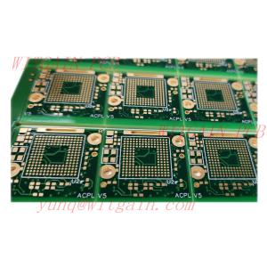
8 Layer Printed Circuit Board With Blind And Buried Holes
PCB Specifications:
Layer Type: HDI PCB
Layer Count: 8 Layer
Board Thickness: 1.6MM
Material: FR4 EM370 EM-370(D) Datasheet 20171121_18061416999.pdf
Min Hole: 0.1MM
Min Line: 4/ Mil
BGA Size: 11Mil
Unit Size: 120MM*112MM/20UP
Blind Holes: L1-L3 , L6-L8 0.1MM
Buried Holes: L3-L6 0.2MM
Via Holes: L1-L8 0.2MM
Solder Mask: Green
Surface Treatment: ENIG
Our Capability:
| NO | Item | Capability |
| 1 | Layer Count | 1-24 Layers |
| 2 | Board Thickness | 0.1mm-6.0mm |
| 3 | Finished Board Max Size | 700mm*800mm |
| 4 | Finished Board Thickness Tolerance | +/-10% +/-0.1(<1.0mm) |
| 5 | Warp | <0.7% |
| 6 | Major CCL Brand | KB/NanYa/ITEQ/ShengYi/Rogers Etc |
| 7 | Material Type | FR4,CEM-1,CEM-3,Aluminum,Copper, Ceramic, PI, PET |
| 8 | Drill Hole Diameter | 0.1mm-6.5mm |
| 9 | Out Layer Copper Thickness | 1/2OZ-8OZ |
| 10 | Inner Layer Copper Thickness | 1/3OZ-6OZ |
| 11 | Aspect Ratio | 10:1 |
| 12 | PTH Hole Tolerance | +/-3mil |
| 13 | NPTH Hole Tolerance | +/-1mil |
| 14 | Copper Thickness of PTH Wall | >10mil(25um) |
| 15 | Line Width And Space | 2/2mil |
| 16 | Min Solder Mask Bridge | 2.5mil |
| 17 | Solder Mask Alignment Tolerance | +/-2mil |
| 18 | Dimension Tolerance | +/-4mil |
| 19 | Max Gold Thickness | 200u'(0.2mil) |
| 20 | Thermal Shock | 288℃, 10s, 3 times |
| 21 | Impedance Control | +/-10% |
| 22 | Test Capability | PAD Size min 0.1mm |
| 23 | Min BGA | 7mil |
| 24 | Surface Treatment | OSP, ENIG,HASL, Plating Gold, Carbon Oil,Peelable Mask etc |
FAQ:
Question: What is Outgassing on a PCB?
Answer: PCB Outgassing is a wave soldering defect in which air is trapped within a PCB during production The air forms voids or blowholes which can degrade the performance of the PCB. This happens during the Wave/ Hand soldering process and when the board is placed in a high-vacuum environment. Outgassing in PCBs usually occurs due to wrong material selection and Faulty manufacturing.
During wave/hand soldering, any moisture close to the through hole is converted into vapor due to the application of heat and whenever this vapor/gas releases, it creates voids in the solder mask layer. When it happens due to soldering, the solder mask voids appear in the electroless copper plating. We all know that plated vias are created conduct current from one board layer to another. When void occurs, it disrupts the smooth current flow, resulting in a defective PCB.
Outgassing can also be caused in a high vacuum environment, like a lab or medical facility. This environment can cause the vapor to release. In a vacuum environment, say space applications, the released vapor can condense on a device like a Camera or some other measurement tool. These condensed particles look like fog and can hinder the measurement results. Some medical facilities also require a vacuum environment, so this problem can arise here as well. Outgassing can contaminate the equipment being used, putting a patient’s life in danger with inaccurate testing results or a foggy screen.
How can PCB Outgassing be prevented?
- Directing the gas away by providing a specific path, where they can do little harm.
- Designers can also use heating elements to burn off the vapour by preventing its deposition on the sensitive apparatus.
- PCBs can be backed before integrating into the system. The baking process can help to get rid of the moisture present on the board.
- Proper through hole plating is recommended. A minimum of 25µm of copper should be present on the surface of the hole walls.
Material evaluation check for PCB Outgassing
As outgassing is prominent in the PCBs used in space equipment, NASA has developed a test procedure called SP-R-0022A to evaluate materials for outgassing. This test procedure has been developed for testing composite materials such as circuit-board laminates.
ASTM International has also proposed the ASTM E595-07 test procedure for assessing material parameters such as TML (total mass loss) and CVCM (Collected Volatile Condensable Material). It evaluates the changes in mass that different materials experience in vacuum environments say during outgassing. During the ASTM process, the test sample is placed in a vacuum at a temperature of 125°C for 24 hours. NASA considers materials only if its TML is less than 1% and the CVCM is less than 0.1%.
After the 24-hour period, the sample is weighed at 23°C. This minimizes the effects of water vapor on the accuracy of the measurement. The samples are weighed consistently within a 2-minute period so that loss of absorption of water vapor is minimized as the sample is exposed to an uncontrolled environment. Sometimes, a WVR (Water Vapor Recovered) test is also performed.


Blind Buried Holes FR4 EM370 8 Layer HDI PCB Board
Inquiry Cart
0