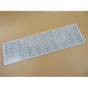
HASL UL 94-V0 Aluminum Based PCB Dual Layer 2.1mm
Brand Name:Bicheng
Certification:UL, ISO9001, IATF16949
Model Number:BIC-751.V1.0
Minimum Order Quantity:1PCS
Delivery Time:8-9 working days
Payment Terms:T/T
Contact Now
Add to Cart
Verified Supplier
Location:
Shenzhen Guangdong China
Address:
6-11C Shidai Jingyuan,Fuyong, Baoan, Shenzhen, Guangdong, China 518103
Supplier`s last login times:
within 1 hours
Product Details
Company Profile
Product Details
Double Layer Aluminum Printed Circuit Board Dual Layer Aluminum Based PCB 2-Layer MCPCB
1.1 Data Sheet
| PCB SIZE | 500 x 150mm=10PCS |
| BOARD TYPE | IMS mcpcb |
| Number of Layers | Double sided PCB, Metal core PCB |
| Surface Mount Components | YES |
| Through Hole Components | NO |
| LAYER STACKUP | copper ------- 70um(2oz) |
| dielectric material 75um | |
| copper ------- 70um(2oz) | |
| dielectric material 75um | |
| Aluminum backed 1.8mm | |
| TECHNOLOGY | |
| Minimum Trace and Space: | 5.98mil/6.18mil |
| Minimum / Maximum Holes: | 0.3/2.2mm |
| Number of Different Holes: | 5 |
| Number of Drill Holes: | 548 |
| Number of Milled Slots: | 11 |
| Number of Internal Cutouts: | 0 |
| Impedance Control | no |
| BOARD MATERIAL | |
| Thermal conductivity | 2W / MK |
| Final foil external: | 2oz |
| Final foil internal: | 2oz |
| Final height of PCB: | 2.1mm ±0.2 |
| PLATING AND COATING | |
| Surface Finish | Hot Air Soldering Leveling(HASL),lead free, Sn>=2.54µm |
| Solder Mask Apply To: | Top, 12micon Minimum. |
| Solder Mask Color: | Super White for LED |
| Solder Mask Type: | LPSM |
| CONTOUR/CUTTING | Routing |
| MARKING | |
| Side of Component Legend | TOP |
| Colour of Component Legend | Black |
| Manufacturer Name or Logo: | Marked on the board in a conductor and leged FREE AREA |
| VIA | via tented. |
| FLAMIBILITY RATING | UL 94-V0 Approval MIN. |
| DIMENSION TOLERANCE | |
| Outline dimension: | 0.0059" (0.15mm) |
| Board plating: | 0.0030" (0.076mm) |
| Drill tolerance: | 0.002" (0.05mm) |
| TEST | 100% Electrical Test prior shipment |
| TYPE OF ARTWORK TO BE SUPPLIED | email file, Gerber RS-274-X, PCBDOC etc |
| SERVICE AREA | Worldwide, Globally. |
1.2 Layer up
The most common MCPCB construction consists of the following 3
layers:
1) A metal substrate, typically aluminum. In some applications, a copper substrate is more appropriate due to its high thermal conductivity than aluminum (401W/MK versus 237 W/MK) but more expensive.
2) Epoxy dielectric layer. This is the most important layer in the MCPCB construction as it affects the thermal performance, electrical breakdown strength, and, in some cases, the solder joint performance of the MCPCB system. The typical thermal conductivity of the dielectric layer on a MCPCB is 1W/MK. A higher value is better for good thermal performance. A thinner dielectric layer is better for thermal performance as well but can negatively impact the ability of the MCPCB to withstand a high potential test to meet minimum electrical safety standards as required in certain lighting markets. The typical dielectric thickness layer is 100μm.
3) Top copper layer. A thicker copper layer improves heat spreading into the PCB but may pose challenges for PCB manufacturers when fabricating narrow traces or spaces. A copper thickness of 1oz (35μm) or 2oz (70μm) is common.
1.3 Metal Core PCB Capability 2021
| NO. | Parameter | Value |
| 1 | Type of Metal Core | Aluminum, Copper, Iron |
| 2 | Model of Metal Core | A1100, A5052, A6061, A6063, C1100 |
| 3 | Surface Finish | HASL, Immersion Gold, Immersion Silver, OSP |
| 4 | Thickness of Surface plating | HASL: Sn>2.54µm, ENIG: Au 0.025-0.1µm, Ni 2.5-5µm |
| 5 | Layer Count | 1-2 Layers |
| 6 | Maximum of Board Size | 23" x 46" (584mm×1168mm) |
| 7 | Mininum of Board Size | 0.1969" x 0.1969" (5mm×5mm) |
| 8 | Board Thickness | 0.0157" x 0.2362" (0.4-6.0mm) |
| 9 | Copper Thickness | 0.5OZ(17.5µm),1OZ(35µm),2OZ(70µm),3OZ(105µm),4OZ(140µm) to 10oz (350µm) |
| 10 | Minimum Track Width | 5mil (0.127mm) |
| 11 | Minimum Space | 5mil (0.127mm) |
| 12 | Minimum Hole Size | 0.0197" (0.5mm) |
| 13 | Maximum Hole Size | No limit |
| 14 | Minimum Holes Punched | PCB thickness <1.0mm: 0.0394" (1.0mm) |
| PCB thikness 1.2-3.0mm: 0.0591" (1.5mm) | ||
| 15 | PTH Wall Thickness | >20µm |
| 16 | Tolerance of PTH | ±0.00295" (0.075mm) |
| 17 | Tolerance of NPTH | ±0.00197" (0.05mm) |
| 18 | Deviation of Hole Position | ±0.00394" (0.10mm) |
| 19 | Outline Tolerance | Routing: ±0.00394" (0.1mm) |
| Punching: ±0.00591" (0.15mm) | ||
| 20 | Angle of V-cut | 30°, 45°, 60° |
| 21 | V-cut Size | 0.1969" x 47.24" (5mm×1200mm) |
| 22 | Thickness of V-cut Board | 0.0236" x 0.1181" (0.6-3mm) |
| 23 | Tolerance of V-cut Angle | ±5º |
| 24 | V-CUT Verticality | ≤0.0059" (0.15mm) |
| 25 | Minimum Square Slots Punched | PCB thickness < 1.0mm: 0.0315" x 0.0315" (0.8 x 0.8mm) |
| PCB thickness 1.2-3.0mm: 0.0394" x 0.0394" (1.0 x 1.0mm) | ||
| 26 | Minimum BGA PAD | 0.01378" (0.35mm) |
| 27 | Minimum Width of Solder Mask Bridge. | 8mil (0.2032mm) |
| 28 | Minimum Thickness of Solder Mask | >13µm (0.013mm) |
| 29 | Insulation Resistance | 1012ΩNormal |
| 30 | Peel-off Strength | 2.2N/mm |
| 31 | Solder float | 260℃ 3min |
| 32 | E-test Voltage | 50-250V |
| 33 | Thermal Conductivity | 0.8-8W/M.K |
| 34 | Warp or Twist | ≤0.5% |
| 35 | Flammability | FV-0 |
| 36 | Minimum Height of Component indicator | 0.0059"(0.15mm) |
| 37 | Minimum Open Solder Mask on Pad | 0.000394" (0.01mm) |


HASL UL 94-V0 Aluminum Based PCB Dual Layer 2.1mm
Inquiry Cart
0