
Add to Cart
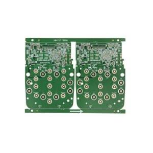
10 Layer HDI Prinred Circuit Boards FR4 TG170 Green Soldermask High Density HDI PCB Manufacturer
Company Profile:
Abis Circuits Co., Ltd is a professional PCB manufacturer in China, Shenzhen. With 14 years+ development, we could make the PCB from 1L to 20L, with a monthly production capability of 60,000 square meters. Abis Circuits is providing high-quality bare PCB and PCB assembly service, including components sourcing, function test, conformal coating, and complete assembly for clients all over the world, Our main market is Europe, north USA, Australia, South America, and Asia.
More than 4 years of working experience for technical backbone, 85% of front-line operation staff, more than 3 years of working experience.
Operation plant space:
(I) 10000 Square meters
(II) 60000 Square meters
Employees:
(I) 300 Man Powers
(II) 900 Man Powers
Eng. Technical:
(I) 20 QA QC Engineers
(II) 60 QA QC Engineers
Product Description
| Item | Spec |
| Layers | 1~20 |
| Board Thickness | 0.1mm-8.0mm |
| Material | FR-4, CEM-1/CEM-3, PI, High Tg, Rogers, PTEF, Alu/Cu Base, etc |
| Max Panel Size | 600mm×1200mm |
| Min Hole Size | 0.1mm |
| Min Line Width/Space | 3mil(0.075mm) |
| Board Outline Tolerance | 士0.10mm |
| Insulation Layer Thickness | 0.075mm--5.00mm |
| Out Layer Copper Thickness | 18um--350um |
| Drilling Hole (Mechanical) | 17um--175um |
| Finish Hole (Mechanical) | 0.10mm--6.30mm |
| Diameter Tolerance (Mechanical) | 0.05mm |
| Registration (Mechanical) | 0.075mm |
| Aspect Ratio | 16:01 |
| Solder Mask Type | LPI |
| SMT Mini. Solder Mask Width | 0.075mm |
| Mini. Solder Mask Clearance | 0.05mm |
| Plug Hole Diameter | 0.25mm--0.60mm |
| Impedance Control Tolerance | 士10% |
| Surface finish | ENIG, OSP, HASL, Chem. Tin/Sn, Flash Gold |
| Soldermask | Green/Yellow/Black/White/Red/Blue |
| Silkscreen | Red/Yellow/Black/White |
| Certificate | UL, ISO 9001, ISO14001, IATF16949 |
| Special Request | Blind hole, Gold finger, BGA, Carbon ink, peekable mask, VIP process, Edge plating, Half holes |
| Material Suppilers | Shengyi, ITEQ, Taiyo, etc. |
| Common Package | Vacuum+Carton |
Hot sales Product Description
| Production capacity of hot-sale products | |
| Double Side/Multilayer PCB Workshop | Aluminum PCB Workshop |
| Technical Capability | Technical Capability |
| Raw materials: CEM-1, CEM-3, FR-4(High TG), Rogers, TELFON | Raw materials: Alurminum base, Copper base |
| Layer: 1 layer to 20 Layers | Layer: 1 layer and 2 Layers |
| Min.line width/space: 3mil/3mil(0.075mm/0.075mm) | Min.line width/space: 4mil/4mil(0.1mm/0.1mm) |
| Min.Hole size: 0.1mm(dirilling hole) | Min.Hole size: 12mil(0.3mm) |
| Max. Board size: 1200mm* 600mm | Max.Board size: 1200mm* 560mm(47in* 22in) |
| Finished board thickness: 0.2mm- 6.0mm | Finished board thickness: 0.3~ 5mm |
| Copper foil thickness: 18um~280um(0.5oz~8oz) | Copper foil thickness: 35um~210um(1oz~6oz) |
| NPTH Hole Tolerance: +/-0.075mm, PTH hole Tolerance: +/-0.05mm | Hole position tolerance: +/-0.05mm |
| Outline Tolerance: +/-0.13mm | Routing outline tolerance: +/ 0.15mm; punching outline tolerance:+/ 0.1mm |
| Surface finished: Lead free HASL, immersion gold(ENIG), immersion silver, OSP, gold plating, gold finger, Carbon INK. | Surface finished: Lead free HASL, immersion gold(ENIG), immersion silver, OSP etc |
| Impedance control tolerance: +/-10% | Remain thickness tolerance: +/-0.1mm |
| Production capability: 50,000 s.q.m/month | MC PCB Production capability: 10,000 s.q.m/month |
Lead Time
| Category | Quickest Lead Time | Normal Lead Time | |
| Double sideds | 24hrs | 120hrs | |
| 4 Layers | 48hrs | 172hrs | |
| 6 Layers | 72hrs | 192hrs | |
| 8 Layers | 96hrs | 212hrs | |
| 10 Layers | 120hrs | 268hrs | |
| 12 Layers | 120hrs | 280hrs | |
| 14 Layers | 144hrs | 292hrs | |
| 16-20 Layers | Depends on the specific requirements | ||
| Above 20 Layers | Depends on the specific requirements | ||
PCB Manufacturing Process
- The process starts with designing Layout of the PCB using any PCB designing software / CAD Tool (Proteus, Eagle, Or CAD).
- All rest of the steps are of Manufacturing Process of a Rigid Printed Circuit Board is same as Single Sided PCB or Double Sided PCB or Multi-layer PCB.
FAQ
Q1:When can I get the quotation?
A:We usually quote with 1 hour after we get your inquiry. If you are
very urgent, please call us or tell us in your email.
Q2:I am a small wholesaler, do you accept small order?
A:It's no problem. If you're small wholesaler, we would like to grow
up with you together.
Q3:How many days will samples be finished? And how about the mass
production?
A:Generally 2-3 days for samples making. The lead time of mass
production will depend on the order quantity and the season you
place the order.
Q4:If I order big quantity, what's the good price?
A: Please send the details enquiry to us, such as the Item Number,
Quantity for each item, Quality request, Logo, Payment Terms,
Transport method, Discharge place etc. We will make the accurate
quotation to you as soon as possible.
Q5: How can we know the processing about PCB order?
A: Each Customer will have a sale to contact with you. Our working
hours: AM 9:00-PM 19:00(Beijing Time) from Monday to Friday. We
will reply your email as soon as quickly during our working time.
And you also could contact with our sales by cellphone if urgent.
Q6:Can I have samples to test?
A: Yes, we are pleased to supply module samples to test and check
quality, mixed sample order is available. Please note buyer should
pay for shipping cost.
Q7:Can you design pcb and make files for us?
A:yes,We have a professional drawing engineers' team that you can
trust.
Q8:If all pcb , PCBs will be tested before delivery if we provide the
function testing method?
A:Yes, we ensure that each piece of pcb, PCBs will be tested before
shipment, we ensure the goods we sent with good quality.
Q9:What is the shipping method?
A:We suggest you using DHL, UPS, FedEX, TNT forwarder.
Q10:How about the payment terms?
A:By T/T, Paypal, Western Union, etc.


