
Add to Cart
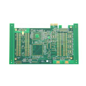
FR4 IT180 94V0 RoHS 2-4u" ENIG Multi Layer PCB HDI Printed Circuit
Board
Abis Circuits Co., Ltd is a professional PCB manufacturer which was
established on Oct, 2006 and focus on double side, Multilayer and
HDI pcb mass production.
We have two factories together , the factory in Shenzhen is
specialized in small and middle volume orders and the factory in
Huizhou is for big volume and HDI.
Product Details:
What is a HDI PCB?
IPC-2226 defines HDI as a printed circuit board with a higher
wiring density per unit area than conventional printed circuit
boards (PCB). They have finer lines and spaces ≤ 100 µm / 0.10mm,
smaller vias (<150 µm) and capture pads <400 µm / 0.40mm, and
higher connection pad density (>20 pads/cm2) than employed in
conventional PCB technology.
Products Information:
| Number of layers | 4 – 22 layers standard, 30 layers advanced |
| Technology highlights | Multilayer boards with a higher connection pad density than standard boards, with finer lines/spaces, smaller via holes and capture pads allowing microvias to only penetrate select layers and also be placed in surface pads. |
| HDI builds | 1+N+1, 2+N+2, 3+N+3,4+N+4, any layer in R&D |
| Materials | FR4 standard, FR4 high performance, Halogen free FR4, Rogers |
| Copper weights (finished) | 18μm – 70μm |
| Minimum track and gap | 0.075mm / 0.075mm |
| PCB thickness | 0.40mm – 3.20mm |
| Maxmimum dimensions | 610mm x 450mm; dependant upon laser drilling machine |
| Surface finishes available | OSP, ENIG, Immersion tin, Immersion silver, Electrolytic gold, Gold fingers |
| Minimum mechanical drill | 0.15mm |
| Minimum laser drill | 0.10mm standard, 0.075mm advanced |
Capacity:
| Via Plugging (100% Fill) | –20% |
| Via Size | ≤0.50mm |
| Registration | 0.025mm |
| Solder Dam Width | Min. 0.15mm |
| Thickness Over Trace (Surface) | Min. 10µm |
| Solder Mask Pad Size | Min. 15µm |
| Maximum board thickness | 6.00mm |
| Minimum board thickness | 0.30mm |
| Minimum Track / Gap Inner layer | 0.075mm |
| Minimum Track / Gap Outer layer (35µm) | 0.075mm |
| Finished PCB Thickness | ±10% |
| Routing Profile | ±0.15mm |
| V-Cut profile | ±0.15mm |
| AOI | All Multilayer |
| Impedance Control | ± 10% |
| Solderability Testing | As standard |
| Ionic Contamination | On Request |
Lead time:
| Board Type | Manufacturing Lead Time |
| Single Sided | 5 – 20 Days dependant on volume |
| PTH | 7 – 25 Days dependant on volume |
| Multilayer | 15 – 30 Days dependant on volume & Technology |
·
| Air Freight Lead Time – 4 Days |
| Sea Freight Lead Time – 30 Days |
| All Far East lead times are subject to customs clearance |
| Premium International shipments can be arranged by DHL, Fedex, UPS or TNT at extra cost |
Our mission:
PCBs for demanding customers, on time with zero defects, produced
sustainably at the lowest total cost. Manufacturing many different
types of PCBs in smaller series (High-mix, Low-volume) involves
constantly adjusting, adapting and problem solving.
Our responsibility:
We know that the PCB is a critical key component for our customers.
And we know for sure that anything can happen during the complex
production process involved – and it often does. In our world,
taking full responsibility means a lot of things, including a
responsible and sustainable approach in everything we do –
socially, environmentally and ethically. When a problem occurs, we
try as hard as we can to understand the problem and find a
solution. Our mindset is that we own the problem and don’t leave
until we have cleared it up.
PCBs we made:
Factory:
Workshop:


