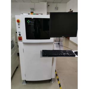
The KY8030 SPI machine is a specialized equipment used in the
electronics manufacturing industry for solder paste inspection
(SPI) during the surface mount technology (SMT) assembly process.
It offers advanced features and capabilities that ensure accurate
and efficient inspection of solder paste deposits on printed
circuit boards (PCBs) before component placement.
Product feature:
-Full 3D measurement and inspection solutions
- Solve shadow issues by using bidirectional projection
- Full 3D foreign object detection solution, applicable to the
entire PCB
- Provides accurate inspection data with real-time PCB deformation
compensation
-Process optimization solution based on full 3D data: realizing
Industry 4.0/Smart Factory
- Real-time process optimization through powerful SPC analysis
- Provides powerful printing process optimization tools
- A leading model suitable for high-speed high-volume production
lines
| Product name | SPI |
| Brand | KOH YOUNG |
| Model | KY8030 |
| Solve the shadow problem | Shadow-eliminating Moldo-stripe technology Bi-directional
illumination light system |
| Real-time compensation of plate bending (2D+3D solution) | plate bending compensation (z+Tracking+Pad Referencing) |
| Easy to operate | Renewal GUL+Pad Referencing. |
| Easy to inspect | 2mm(4 Way Projection) |
| Foreign body inspection | 3D foreign object inspection function |
| Inspction item | volume, area, offset, bridge, shape, coplanarity |
| Max inspection size | 10*10mm 0.39*0.39inches |
| Max inspection height | 400um |
| Minimum pad pitch | 100um(150mm Solder paste height) |
| Corresponding to various color substrates | yes |
| Rail width adjusted | Auto |
| Fix rail | front rail fixed, rear rail fixed. |
Functionality:
1. High-Resolution Imaging: The KY8030 SPI machine utilizes
high-resolution imaging technology to capture detailed images of
the solder paste deposits on the PCB. This imaging capability
enables precise inspection and measurement of paste volume, shape,
and alignment.
2. 3D Inspection: The machine is equipped with a 3D inspection
system that utilizes laser or structured light projection to create
a detailed three-dimensional representation of the solder paste
deposits. This allows for accurate height measurement and detection
of defects such as insufficient or excessive solder paste.
3. Automatic Inspection: The KY8030 SPI machine automatically scans
and inspects the solder paste deposits on the PCBs. It compares the
inspected data against predefined specifications and identifies any
deviations or defects in real-time.
4. Inspection Data Analysis: The machine provides comprehensive
data analysis capabilities, including statistical analysis and data
visualization. It allows operators to analyze trends, identify
process variations, and make informed decisions for process
optimization and quality improvement.
5. Intuitive User Interface: The machine is equipped with a
user-friendly interface that allows operators to set up inspection
parameters, define inspection regions, and visualize inspection
results. The interface provides easy-to-understand graphical
representations for quick interpretation of inspection data.
Usage Instructions:
1. Setup: Ensure that the KY8030 SPI machine is properly installed
and connected to the power supply. Calibrate the machine according
to the manufacturer's instructions to ensure accurate measurement
and inspection.
2. PCB Preparation: Prepare the PCBs for inspection by ensuring
that the solder paste is applied accurately and in the appropriate
locations. Verify that the PCBs are clean and free from any
contaminants that may affect the inspection.
3. Programming: Use the machine's interface to set up the
inspection parameters, such as inspection region, threshold values,
and defect detection criteria. Define the inspection requirements
based on the solder paste specifications and assembly process
guidelines.
4. Loading: Place the PCBs onto the inspection stage or conveyor
system of the KY8030 SPI machine. Ensure proper alignment and
fixation to prevent any movement or misalignment during the
inspection process.
5. Inspection: Initiate the inspection process using the machine's
interface. The machine will automatically scan the solder paste
deposits on the PCBs, capturing images and collecting inspection
data. Monitor the inspection results in real-time and identify any
defects or deviations from the predefined specifications.
6. Data Analysis: Analyze the inspection data using the machine's
data analysis tools. Utilize statistical analysis, visualization,
and trend monitoring to identify process variations and take
appropriate corrective actions if necessary.
7. Reporting: Generate inspection reports that summarize the
inspection results, including defect analysis, statistical data,
and visual representations. These reports can be used for process
improvement and documentation purposes.
8. Maintenance: Regularly clean the machine's imaging system and
inspection stage to ensure accurate and reliable performance.
Follow the manufacturer's maintenance guidelines for any required
calibration or component replacement.
The KY8030 SPI machine offers advanced capabilities for accurate
solder paste inspection in electronic manufacturing. By following
the proper setup and usage instructions, it enables efficient
process control and quality assurance in the SMT assembly process.