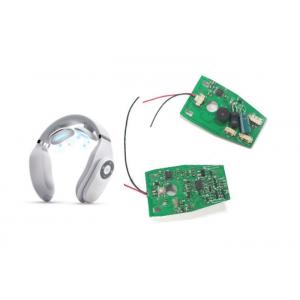
Designing Pcb Boards Multilayer Pcb Design Electronics Pcb Design Layout
Brand Name:YDY
Certification:ISO13485, IATF16949, ISO9001
Model Number:PD-4
Minimum Order Quantity:1pcs
Delivery Time:1-10 working days
Payment Terms:L/C, D/A, D/P, T/T, Western Union, MoneyGram
Contact Now
Add to Cart
Active Member
Location:
Shenzhen China
Address:
深圳市宝安区福永凤凰西区202号信诺大厦401
Supplier`s last login times:
within 27 hours
Product Details
Company Profile
Product Details
Designing Pcb Boards Multilayer Pcb Design Electronics Pcb Design Layout
Whether you need hardware design, software development or one- stop
product development, YDY can provide you with high-quality design
services. Our team consists of many experienced electronic
engineers, Covers FGPA antenna design, chip design and so on. YDY,
always your first choice for PCB design .
I can help you with your product development needs. Either from the
start or as additional engineering resources for your engineering
division. YDY services are used by both local and international
companies, with today's modern communications location is no
barrier.
What we need for design&layout?
1) Schematics(.DSN and .SCH suffixes )
2) DXF structure drawing (2D drawing in AutoCAD format, used to
position the device and build board size)
3) The component specification (the specification must be with the
device size diagram for the establishment and physical one-to-one
corresponding package
4) Special requirements
PCB capability :
| Service | YDY is a product development company specialising in electronic design and product development. Its principle Mark Barber has been involved in electronic design and product development for more than 25 years. With degrees and qualifications in electronics, communication, C programming, CPLD, VHDL, Visual Studio and other areas, a solid knowledgeable background is always a must. |
| Schematic Diagram Design | Our team consists of experienced engineers, such as FPGA senior engineers, antenna experts ect. No matter how complicated the project is, our engineers can design the schematic diagram to meet your requirements. |
| PCB Design and Layout | We use different PCB design softwares to meet your needs: Altium Designer; Cadence Orcad or Allegro; Eagle; KiCAD, which provides very high level PCB design files and full 3D CAD design output capabilities. |
| Algorithm Development | If you meet algorithm problem, we can help you solve it. Our algorithm engineer has rich experience in image processing, data processing and so on. |
| Shape | Retangular, Round, Slots, Cutouts, Complex, Irregular |
| Cutting | Shear, V-score, Tab-routed |
| Board Thickness | 0.2-4mm, regular 1.6mm |
| Copper Thickness | 0.5-4oz, regular 1oz |
| Solder Mask | Green, Red, Blue, Yellow, etc. |
| Silk Screen | White, Black, etc. |
| Silk Screen Min Line Width | 0.006" or 0.15mm |
| Min Trace/Gap | 0.1mm or 4mils |
| Min Drill Hole Diameter | 0.01",0.25mm or 10mils |
| Surface Finish | HASL, ENIG, OSP, etc. |
Shenzhen Yideyi Technology Co., Ltd is an electronic designer that
lets printed circuit board (PCB) designers seamlessly connect
schematic diagrams, component placement, PCB routing, and
comprehensive library content.
Our advantage :
1. we have our own PCBA factory with more than 12 SMT production
line.
2. We can Customize The Product According To Your Idea and turn it
into final products.
3. OEM&ODM electronic design, industrial design and mechanical
design experience from mold design to manufacturing with one-stop
service
4. Our designers and engineers all use AUTO CAD,Pro/E,UG and
Soliworks software to check 2D and 3D drawings.


Designing Pcb Boards Multilayer Pcb Design Electronics Pcb Design Layout
Inquiry Cart
0