
Add to Cart
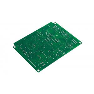
60 Layers Hdi Pcb Board Sequential Lamination Stacked Microvias
Our HDI PCB Board Capabilities include:
High Thermal Reliability
Ultra-Low Loss
High Speed Digital
Halogen-Free
RoHS Compliant
Lead-Free High Tg
| Feature | Capability |
| Service Type | 60 Layers Hdi Pcb Board Sequential Lamination Stacked Microvias |
| Quality Grade | Standard IPC 2 |
| Number of Layers | 4 - 48ayers |
| Order Quantity | 1pc - 10000+pcs |
| Build Time | 2days - 5weeks |
| Material | FR4 standard Tg 140°C,FR4 High Tg 170°C, FR4 and Rogers combined lamination |
| Board Size | Min 6*6mm | Max 457*610mm |
| Board Thickness | 0.4mm - 3.0mm |
| Copper Weight (Finished) | 0.5oz - 2.0oz |
| Min Tracing/Spacing | 2.5mil/2.5mil |
| Solder Mask Sides | As per the file |
| Solder Mask Color | Green, White, Blue, Black, Red, Yellow |
| Silkscreen Sides | As per the file |
| Surface Finish | HASL - Hot Air Solder Leveling Lead Free HASL - RoHS ENIG - Electroless Nickle/Immersion Gold - RoHS Immersion Silver - RoHS Immersion Tin - RoHS OSP - Organic Solderability Preservatives - RoHS |
| Min Annular Ring | 4mil, 3mil - laser drill |
| Min Drilling Hole Diameter | 6mil, 4mil - laser drill |
| Max Exponents of Blind/Buried Vias | stacked vias for 3 layers interconnected, staggered vias for 4 layers interconnected |
| Other Techniques | Flex-rigid combination Via In Pad Buried Capacitor (only for Prototype PCB total area ≤1m²) |
What is HDI PCB?
High-Density Interconnect (HDI) is simply a PCB with more number of
interconnections, occupying minimal space. This results in the
miniaturization of the circuit board. The components are placed
closer and the board space is significantly reduced but the
functionality isn’t compromised.
To be more precise, a PCB with an average of 120 to 160 pins per square inch is considered as an HDI PCB.
The HDI design incorporates dense component placement and versatile routing. The HDI popularized microvia technology. A denser circuitry is crafted with the implementation of microvias, buried vias, and blind vias. The drill to copper is reduced in an HDI design.
Shenzhen Yideyi Technology Co., Ltd can supply PCB, PCBA, Gerber design, Clone, one stop OEM and ODM service.
FAQs:
1, Do you offer quick turn PCB Assembly ?
Yes, we offer 24 hours quick turn PCB Assembled Solution without
sacrifice the quality of the PCB Board.
2, Do you offer X-Ray capability ?
Yes, we inspect the boards using X-ray and therefore offer total
reliability.
3, Do you offer conformal coating service ?
Yes, conformal coating is a part of our value-added services.
4, Do you offer testing service ?
Yes, we offer robust functional testing that adds to the product
reliability.
5, Do you offer IPC 610 or J-STD Quality inspections ?
Absolutely, we offer these inspections as per client requirements.
6, Do you offer first article inspection ?
Yes, basis client requirements, we are well equipped to offer first
article inspection.
7, What is your standard turnatound time for PCB Assembly ?
Our standard turnaround time for PCB Assembly is 3 weeks.
8, What file formats do you accept for production?
Gerber file: CAM350 RS274X
PCB file: Protel 99SE, P-CAD 2001 PCB
BOM: Excel (PDF,word,txt)


