
Add to Cart
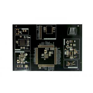
0.2mm COB Rigid-Flex Double-Sided Printed Multilayer PCB Bare Board
Shenzhen Yideyi Technology Co., Ltd is located in the beautiful scenery of Shenzhen city of Guangdong Province, it has modernized standard workshop of 9000 square meters, more than 500 employees, is a professional manufacturers of production of aluminum plate, single, double, multilayer printed circuit board and flexible circuit board.
We have a strong engineering team, high quality and efficient production and fast and global service in the industry are in a leading position, based on quality, service, efficiency and win-win, our processing products are widely used in computer, communication, auto parts products, medical equipment, precision instruments, aviation equipment, and other fields, we also provide the OEM service to customers in Europe and America, South Korea, Japan, Southeast Asia, the Middle East and Latin America. Companies adhering to thought of the “management of science and technology and creative enterprise”, continue develop new process and new products so that ahead of competition in the market. The perfect quality management system can provide a solid guarantee for us to produce high quality products. Our company can provide copy board, sample, mass production service, and provide the express production services for the customers and so on.
Multilayer PCB Benefits:
From a technical point of view, multilayer PCBs present several advantages in design. These benefits multilayer PCBs present include:
• High-Quality: Due to the amount of work and planning that must go into the creation of multilayer PCBs, these types of PCBs tend to be better in quality than single and double-layer PCBs. They also tend to be more reliable as a result.
• Increased Durability: Multilayer PCBs tend to be durable by their nature. Not only do these multilayer PCBs have to withstand their own weight, but they must also be able to handle the heat and pressure used to bind them together. On top of these factors, multilayer PCBs use multiple layers of insulation between circuit layers, binding it all together with prepreg bonding agent and protective materials.
• Enhanced Flexibility: Though this does not apply to all multilayer PCB assemblies, some do use flexible construction techniques, resulting in a flexible multilayer PCB. This can be a highly desirable trait for applications where mild bending and flexing may occur on a semi-regular basis. Again, this does not apply to all multilayer PCBs, and the more layers incorporated into a flexible PCB, the less flexible the PCB becomes.
• More Powerful: Multilayer PCBs are extremely high-density assemblies, incorporating multiple layers into a single PCB. These close-quarters enable boards to be more connective, and their innate electrical properties allow them to achieve greater capacity and speed despite their smaller size.
• Single Connection Point: Multilayer PCBs are designed to work as a singular unit, rather than in tandem with other PCB components. As a result, they have a single connection point, rather than the multiple connection points required to use multiple single layer PCBs. This proves to be a benefit in electronic product design as well since they only need to include a single connection point in the final product. This is particularly beneficial for small electronics and gadgets designed to minimize size and weight.
These benefits make multilayer PCBs highly useful in a variety of applications, particularly mobile devices and high-functioning electronics. In turn, with so many industries turning to mobile solutions, multilayer PCBs are finding a place in an increasing number of industry-specific applications.
Our service
1. SMT service;
2. Design service, Gerber drawings;
3. Good quality and fast delivery with lower price than double side PCB.
4. Specifications of LEAD Free HASL 1 Layer / Single Side Rigid PCB/PCBA:
1) Base material: FR-1(94v0), FR-4, CEM-1,
2) Max Board size: 600*600mm
3) Board thickness: 0.2mm/0.6mm/0.8mm/1.2mm/1.6mm/3.2mm
4) Copper thickness: 0.5oz , 1oz , 2oz ,3oz,4oz, 5oz ,7oz , 11oz
5) Special tech: BGA, PTH, Blind and buried vias
6) Profile: V-scoring, V-cutting, punching, etching, milling, routing
7) Surface treatment: HASL, OS, Immersion gold, gold plated (coating)
8) With best price to USA, South American, India, South Africa and Europe
9) Main market: USA, EGYPT, Europe, South American, mid-east
10) Compliant: UL, ROHS, ISO9001-2000
11) Standard: IPC-A-600F, IPC-D-300G, MIL-STD-105D LEVEL II
12) Application: Home appliances, electronics, digital camera, LCD TV sets, medical equipments, telecommunication, LED lightings, street light, mobile phone, computer, laptop test equipment and power meter, electrical weighing scale, night
13) Small quantity and prototypes acceptable
14) Lead time: 5-7days for prototypes, 9-13days for mass production
15) Available Service: OEM, 24hrs service for fast prototype
SMT Production processes:
Material Receiving → IQC → Stock → Material to SMT → SMT Line Loading → Solder Paste/Glue Printing → Chip Mount → Reflow → 100% Visual Inspection → Automated Optical Inspection (AOI) → SMT QC Sampling → SMT Stock → Material to PTH → PTH Line Loading → Plated Through Hole → Wave Soldering → Touch Up → 100% Visual Inspection → PTH QC Sampling → In-Circuit Test (ICT) → Final Assembly → Functional Test (FCT) → Packing → OQC Sampling → Shipping
PCB Assembly Manufacturing Procedures:
Program Management
PCB Files → DCC → Program Organizing →Optimization → Checking
SMT Management
PCB Loader → Screen Printer → Checking → SMD Placement → Checking → Air Reflow → Vision Inspection → AOI → Keeping
PCBA Management
THT→Soldering Wave (Manual Welding) → Vision Inspection → ICT → Flash → FCT → Checking → Package → Shipment
Files Requested For Quote:
In order to provide you with the most efficient and accurate quote on manufacturing the requested unit, we ask that you provide us with the following information:
1. Gerber file,PCB file,Eagle file or CAD file are all acceptable
2. A detailed bill of materials (BOM)
3. Clear pictures of PCB or PCBA sample for us
4. Quantity and delivery required
5. Test method for PCBA to guarantee 100% good quality products.
6. Schematics file for PCB design if need to do function test.
7. A sample if available for better sourcing
8. CAD files for enclosure manufacturing if required
9. A complete wiring and assembly drawing showing any special assembly instructions if required
| Process | Item | Mass production capability | |
| SMT | Printing | Max PCB size | 900*600mm² |
| Max PCB weight | 8kg | ||
| Solder paste printing tolerance | ±25μm(6σ) | ||
| System repeat calibration tolerance | ±10μm(6σ) | ||
| Scraper pressure detection | pressure closed-loop control system | ||
| SPI | Detect Min BGA PAD to PAD distance | 100μm | |
| x-axis and Y-axis tolerance | 0.5μm | ||
| False Rate | ≤0.1% | ||
| Mount | Component size | 0.3*0.15 mm²--200*125 mm² | |
| Component max height | 25.4mm | ||
| Populate tolerance | ±22μm(3σ),±0.05°(3σ) | ||
| PCB board size | 50*50 mm²-850*560 mm² | ||
| PCB thickness | 0.3mm--6mm | ||
| Populate Max components type | 500 | ||
| AOI | Detect Min components | 01005 | |
| Detect false type | Incorrect conponents,missing components,opposite direction,,component shift,Tombstone,Mounting on side,unsoldering,insufficient solder,Lead raised,Solder ball | ||
| Foot warping detection | 3D Detection function | ||
| Reflow | Temperature Accuracy | ±1ºC | |
| Welding protection | nitrogen protection;(remaining oxygen<3000ppm) | ||
| Nitrogen Control | Nitrogen closed-loop control system,±200ppm | ||
| 3D X-Ray | Magnification | Geometric Magnification;:2000 times;System Magnification:12000times | |
| Resolution | 1μm /nm | ||
| Rotation Angle &Slanting Perspective | Any ±45°+360°rotation | ||
| DIP | Preelaboration | Automatic forming technology | Component Automatic forming |
| DIP | DIP technology | Automatic Insertion machine | |
| Wave soldering | Wave soldering type | Ordinary wave soldering | |
| Inclination angle of transport guide rail | 4--7° | ||
| Temperature accuracy | ±3ºC | ||
| Soldering protection | nitrogen protection | ||
| Non-welding pressure contact technology | Max PCB board size | 800*600mm² | |
| Press down height accuracy | ±0.02mm | ||
| Pressure Range | 0-50KN | ||
| Pressure Accuracy | Standard value:±2% | ||
| Hold time | 0-9.999S | ||
| Conformal coating technology | Max PCB board size | 500*475*6mm | |
| Max PCB board weight | 5kg | ||
| Min Nozzle size | 2mm | ||
| Other characteristic | Conformal coating pressure Programmable control | ||
| ICT test | test level | Device level test,Test hardware connection status. | |
| Test point | >4096 | ||
| Test content | Contact test ,Open/short test,Resistance capacitance test test,diode, triode,mosfet test,No power on hybrid test,Boundary scan chain test,Power on mixed mode test. | ||
| Assembly and test | Production type | TWS | Mass production |
| Gaming controller | Mass production | ||
| Life Watch | Mass production | ||
| FT test | test level | PCB board system level test.Test System function status. | |
| Temperature cycling test | Temperature range | -60ºC--125ºC | |
| Rise/lower temperature rate | >10ºC/min | ||
| Temperature tolerance | ≤2ºC | ||
| Other Reliability test | burn-in test,Drop test, vibration test , Abrasion test ,Key life test. | ||
Trade Terms:
1. Payment: T/T in advance (Western Union , paypal is welcomed)
2. Production lead time 100PCS: 5-7days, 500~1000PCS: 7-10days, above 1000PCS 15-20days.
3. Sample can be delivered in 3days
4. Shipping freight are quoted under your requests
5. Shipping port: Shen zhen,Mainland China
6. Discounts are offered based on order quantities
7. MOQ: 1PCS
Package &Shipping Methods:
1. Vacuum package with silica gel, Carton box with packing belt.
2. By DHL, UPS, FedEx, TNT
3. By EMS
4. By sea for mass quantity according to customer's requirement
We are the smart choice for you and the trusted source at the center of your deal. Welcome the win-win situation together.
FAQ:
Q1. How to keep our product information and design file secret ?
We are willing to sign a NDA effect by customers side local law and
promising to keep customers data in high confidential level.
Q2. What file formats do you accept for production?
Gerber file: CAM350 RS274X
PCB file: Protel 99SE, P-CAD 2001 PCB
BOM: Excel (PDF,word,txt)
Q3. Please note that the following detail will speed up evaluation:
Material:
Board thickness:
Copper thickness:Surface finish:
Solder mask color:
Silkscreen color:
Q4. How to make sure the PCBAs are completely well recieved?
We will pack with aluminum bag, and insert card, up and bottom card
with stable cartons.
Q5. How to ship the PCBAs?
For small packages, we will ship the boards to you by
DHL,UPS,FEDEX,TNT. Door to door service! For mass production, we
could ship by air, by sea.


