
Add to Cart
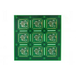
OSP V-Cut Customized Multilayer Printed Circuit Board PCBA Design
Shenzhen Yideyi Technology Co., Ltd have more than 10 years of SMT manufacturing experience, well appointed SMT ,DIP and assembly lines, offering one stop service from SMT,FPC,DIP,EMS, conformal coating, testing, final assembly, component procurement ,design, peripheral products support and so on.
YDY with customers to provide them with the highest-quality PCB and PCBA electronic manufacturing services to achieve their goals. Our flexibility is in meeting customer requirements and our superior customer service. We help companies introduce their new products to market in the fastest time possible by providing high quality, quick-turn assembly.We provide one-stop electronic manufacturing service to help you qualify your designs and provide quality samples to customers.
PCB Capability
| Product Name | Multilayer Printed Circuit Prototype Board PCB Factory |
| Materials | FR-4/HTG150-180 FR-4/CEM-1/CEM-3/Aluminum/F4B-2 |
| Board Thickness | Rigid 0.15mm-3.00mm |
| Board Thickness Tolerance | 5-10% |
| Profile Processing | CNC Milling/V-Cut/Mold Flushes |
| Copper Weight Tolerance | ±0.15 oz |
| Copper Thickness | 0.5oz-5oz |
| Min Line Width | 0.1mm |
| Min Space Width | 0.127mm |
| Min Drill Hole Diameter | 0.1mm |
| Max Processing Sheer | 600mm*400mm |
| Silk Screen Min Line Width | 0.15mm |
| Anti-welds resin | Thermosetting resin/Without the gloss resin/Photosensitive resin |
| Soldermask | green,red,blue,white,black,yellow,etc. |
| Flame resistance | 94v0 |
| Certification | ISO 9001:2000,ISO 14001,ISO/TS16949:2002,UL E203640 |
| Approval Standard | IPC-600F |
| Suface Finish | HASL/Nickle/Lead Free HASL/OSP/Gold Plating/Immersion Gold/ENIG/Rosin etc |
Our One-stop Services:
1. PCB manufacturing service
2. Components sourcing services
3. PCB assembly services
4. Programming & Testing services
5. Housing assembly services
6. Reverse engineering services
7. Cable & wire assembly services
We are the smart choice for you and the trusted source at the center of your deal.
FAQ:
Q1. How to keep our product information and design file secret ?
We are willing to sign a NDA effect by customers side local law and
promising to keep customers data in high confidential level.
Q2. What file formats do you accept for production?
Gerber file: CAM350 RS274X
PCB file: Protel 99SE, P-CAD 2001 PCB
BOM: Excel (PDF,word,txt)
Q3. Please note that the following detail will speed up evaluation:
Material:
Board thickness:
Copper thickness:Surface finish:
Solder mask color:
Silkscreen color:
Q4. How can we guarantee you receive an good quality product?
For PCB, we will use Flying Probe Test, E-test etc. for it.
For PCBA, we need you to offer us a method or test fixture for the
function test.Before that, our inspectors will use microscope and
X-ray to check the IC footwelding or bad solder etc.
Q5. How to ship the PCBAs?
For small packages, we will ship the boards to you by
DHL,UPS,FEDEX,TNT. Door to door service! For mass production, we
could ship by air, by sea.


