
Add to Cart
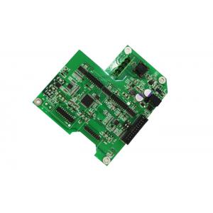
Development Pcb With Gerber File Bom List PCB Soldering Service
PCB Fabrication:
PCBs with up to 14 layers
100% Electrical Testing
Min Track/Spacing 0.1mm/4mil
Min Hole Size:0.2mm
High Density Interconnect PCBs
High-Temp,FR4,Flex,HDI,Rogers,etc
Laser Direct Imaging (LDI)
Special colors & -lacquers
Lead-Free compliant PCBs
Half-cut/Castellated Holes
Edge Plating
Impedance control
PCB capability:
| Specification | |
| Numbr of Layer | 1-18Layers |
| Material | FR-4,FR2.Taconic,Rogers, CEM-1 CEM-3,ceramic , crockery Metal-backed Laminate |
| Surface Finish | HASL(LF), Gold plating, Electroless nickel immersion gold, Immersion Tin, OSP(Entek) |
| Finish Board Thickness | 0.2mm-6.00 mm(8mil-126mil) |
| Copper Thickness | 1/2 oz min;12 oz max |
| Solder Mask | Green/Black/White/Red/Blue/Yellow |
| Min.Trace Width & Line Spacing | 0.075mm/0.1mm(3mil/4mil) |
| Min.Hole Diameter for CNC Driling | 0.1mm(4mil) |
| Min.Hole Diameter for punching | 0.9mm(35mil) |
| Biggest panel size | 610mm*508mm |
| Hole Positon | +/-0.075mm(3mil) CNC Driling |
| Conductor Width(W) | 0.05mm(2mil)or; +/-20% of original artwork |
| Hole Diameter(H) | PTH L:+/-0.075mm(3mil); Non-PTH L:+/-0.05mm(2mil) |
| Outline Tolerance | 0.125mm(5mil) CNC Routing; +/-0.15mm(6mil) by Punching |
| Warp & Twist | 0.70% |
| Insulation Resistance | 10Kohm-20Mohm |
| Conductivity | <50ohm |
| Test Voltage | 10-300V |
| Panel Size | 110×100mm(min);660×600mm(max) |
| Layer-layer misregistration | 4 layers:0.15mm(6mil)max; 6 layers:0.25mm(10mil)max |
| Min.spacing between hole edge to circuity pqttern of an inner layer | 0.25mm(10mil) |
| Min.spacing between board oulineto circuitry pattern of an inner layer | 0.25mm(10mil) |
| Board thickness tolerance | 4 layers:+/-0.13mm(5mil); 6 layers:+/-0.15mm(6mil) |
SMT PCBA capabilities:
• SMT assembly including BGA assembly
• Accepted SMD chips: 01005,BGA,QFP,QFN,TSOP
• Component height: 0.2-25mm
• Min packing: 0201
• Min distance among BGA : 0.25-2.0mm
• Min BGA size: 0.1-0.63mm
• Min QFP space: 0.35mm
• Min assembly size: (X*Y): 50*30mm
• Max assembly size: (X*Y): 350*550mm
• Pick-placement precision: ±0.01mm
• Placement capability: 0805, 0603, 0402, 0201
• High pin count press fit available
How to start order:
Shenzhen Yideyi Technology Co., Ltd offers One-Stop Solution for PCB & Prototype Assembly,specializes in PCB Prototype and small series services. providing high-tech low-cost PCB / multilayer boards with up to 48 layers.For example Impedance Control PCB, Buried & Blind Holes PCB, multilayer-layer PCBs.
FAQ:
Q1. How can we ensure our information should not let third party to
see our design?
We are willing to sign NDA effect by customer side local law and
promising to keep customers date in high confidential level in all
projects.
Q2. What service do you have?
We provide turnkey solution including RD, PCB fabrication, SMT,
final assembly,testing and other value-added service.
Q3. Please note that the following detail will speed up evaluation:
Material:
Board thickness:
Copper thickness:Surface finish:
Solder mask color:
Silkscreen color:
Q4. How about the delivery?
Normally, for sample order, our delivery is about 5 days.For small
batch, our delivery is about 7 days.
For mass production batch, our delivery is about 10 days.
But that depends on the real condition when we get your order.
If your order is urgently please contact us directly ,we will
priority to deal it and do ourbest to give you satisfied delivery
time.
Q5. With payment terms do we accept?
For sample order or small batch, we suggest you to use Pay-pal and
Western Union.For mass production batch, we suggest you to use T/T.
Q6. How can we guarantee you receive an good quality product?
For PCB, we will use Flying Probe Test, E-test etc. for it.
For PCBA, we need you to offer us a method or test fixture for the
function test.Before that, our inspectors will use microscope and
X-ray to check the IC footwelding or bad solder etc.
Q7. What are the main products of your PCB/PCBA service?
Automotive, medical, Industrial control, Internet of Things, Smart home, military, Aerospace.
