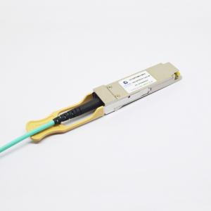
100G QSFP28 Passive Copper Cable 3M AOC Cables Juniper Compatible
Brand Name:OLKOPTO
Certification:RoHS FCC CE GS UL FDA etc
Model Number:OLSQ8TXA-CDM1
Minimum Order Quantity:1pc
Delivery Time:3-5 working days
Payment Terms:T/T or Net 30 days
Contact Now
Add to Cart
Verified Supplier
Location:
Shenzhen China
Address:
4/F, No.2 Building, Delux Science and Technology City, GuanLan Hi-tech park, No.5 Guanyi Road, Longhua District, Shenzhen, China
Supplier`s last login times:
within 23 hours
Product Details
Company Profile
Product Details
100G QSFP28 Passive Copper Cable 3M AOC Cables Juniper Compatible
Juniper Networks Compatible 100G QSFP28 JNP-QSFP28-AOC-3M Active Optical Cable
Description:
QSFP28 Active Optical Cable (AOC) components are designed for 100GB Ethernet applications. It is designed so that 100GbE devices are designed with very high port density based on electrical and mechanical specifications. The application is 100G AOC QSFP28 Applications and 100GBASE-SR4 at 25.781Gbps per lane.
Optical Characteristics (TOP(C) = 0 to 70 ℃, VCC = 3.13 to 3.47 V)
| Parameter | Symbol | Min. | Typ | Max. | Unit | Note |
| Transmitter | ||||||
| Operating Wavelength | λ | 840 | 850 | 860 | nm | |
| Output Optical Eye | Compliant with IEEE 0802.3ae | |||||
| Receiver | ||||||
| Operating Wavelength | 840 | 860 | nm | |||
Electrical Characteristics (TOP(C) = 0 to 70 ℃, VCC = 3.13 to 3.47 V)
| Parameter | Symbol | Min. | Typ | Max. | Unit | Note |
| ModSelL-Module Select | VOL | 0 | 0.8 | V | ||
| ModSelL-Module Unselect | VOH | 2.5 | VCC | V | ||
| LPMode-Low Power Mode | VIL | 0 | 0.8 | V | ||
| LPMode-Normal Operation | VIH | 2.5 | VCC+0.3 | V | ||
| ResetL-Reset | VIL | 0 | 0.8 | V | ||
| ResetL-Normal Operation | VIH | 2.5 | VCC+0.3 | V | ||
| ModPrsL-Normal Operation | VOL | 0 | 0.4 | V | ||
| IntL-Interrupt | VOL | 0 | 0.4 | V | ||
| IntL-Normal Operation | VOH | 2.4 | VCC | V |
| Active cable input electrical characteristics | ||||||
| Differential Data Input Voltage | VIH-VIL | 200 | 1600 | mVpp | 1 | |
| Differential Input Impedance | RIN | 90 | 100 | 110 | Ω | |
| TX-Disable Input Voltage-Low | VIL | 0 | 0.8 | V | 2 | |
| TX-Disable Input Voltage-High | VIH | 2.0 | VCC | V | 2 | |
| TX-Fault Output Voltage-Low | VOL | 0 | 0.8 | V | 3 | |
| TX-Fault Output Voltage-High | VOH | 2.0 | VCC | V | 3 | |
| Active cable output electrical characteristics | ||||||
| Differential Data Output Voltage | VOH- VOL | 200 | 800 | mV | 1 | |
Differential Output Impedance | ROUT | 100 | Ω | |||
LOS-Asserted Output Voltage-Low | VOL | 0 | 0.8 | V | 3 | |
Notes:
1. Average power figures are informative only, per IEEE 802.3ae.
2. Measured at the BER less than 1E-12, back to back. The measure pattern is PRBS 231-1 with worst ER=4.5@ 10.3125Gb/s.
3. Internal AC coupled
4. TX-Disable has an internal 4.7KΩ to 10 KΩ pull-up to VccT
5. Measure with 4.7KΩ pull-up to Vcc on host board
Pin Description
| Pin | Name | Logic | Description | |
| 1 | GND | Ground | 1 | |
| 2 | Tx2n | CML-I | Transmitter Inverted Data Input | 10 |
| 3 | Tx2p | CML-I | Transmitter Non-Inverted Data Input | 10 |
| 4 | GND | Ground | 1 | |
| 5 | Tx4n | CML-I | Transmitter Inverted Data Input | 10 |
| 6 | Tx4p | CML-I | Transmitter Non-Inverted Data Input | 10 |
| 7 | GND | Ground | 1 | |
| 8 | ModSelL | LVTTL-I | Module Select | 3 |
| 9 | ResetL | LVTTL-I | Module Reset | 4 |
| 10 | Vcc Rx | +3.3V Power Supply Receiver | 2 | |
| 11 | SCL | LVCMOS-I/O | 2-wire serial interface clock | 5 |
| 12 | SDA | LVCMOS-I/O | 2-wire serial interface data | 5 |
| 13 | GND | Ground | 1 | |
| 14 | Rx3p | CML-O | Receiver Non-Inverted Data Output | 9 |
| 15 | Rx3n | CML-O | Receiver Inverted Data Output | 9 |
| 16 | GND | Ground | 1 | |
| 17 | Rx1p | CML-O | Receiver Non-Inverted Data Output | 9 |
| 18 | Rx1n | CML-O | Receiver Inverted Data Output | 9 |
| 19 | GND | Ground | 1 | |
| 20 | GND | Ground | 1 | |
| 21 | Rx2n | CML-O | Receiver Inverted Data Output | 9 |
| 22 | Rx2p | CML-O | Receiver Non-Inverted Data Output | 9 |
| 23 | GND | Ground | 1 | |
| 24 | Rx4n | CML-O | Receiver Inverted Data Output | 9 |
| 25 | Rx4p | CML-O | Receiver Non-Inverted Data Output | 9 |
| 26 | GND | Ground | 1 | |
| 27 | ModPrsL | LVTTL-O | Module Present | 6 |
| 28 | IntL | LVTTL-O | Interrupt | 7 |
| 29 | Vcc Tx | +3.3V Power supply transmitter | 2 | |
| 30 | Vcc1 | +3.3V Power supply | 2 | |
| 31 | LPMode | LVTTL-I | Low Power Mode | 8 |
| 32 | GND | Ground | 1 | |
| 33 | Tx3p | CML-I | Transmitter Non-Inverted Data Input | 10 |
| 34 | Tx3n | CML-I | Transmitter Inverted Data Input | 10 |
| 35 | GND | Ground | 1 | |
| 36 | Tx1p | CML-I | Transmitter Non-Inverted Data | |
| 37 | Tx1n | CML-I | Transmitter Inverted Data Input | 10 |
| 38 | GND | Ground | 1 |
Notes:
1. GND is the symbol for signal and supply (power) common for the module. All are common within the module and all module voltages are referenced to this potential unless otherwise noted. Connect these directly to the host board signal-common ground plane.
2. Vcc Rx, Vcc1 and Vcc Tx shall be applied concurrently. Vcc Rx Vcc1 and Vcc Tx may be internally connected within the module in any combination. The connector pins are each rated for a maximum current of 1000 mA. Recommended host board power supply filtering is shown below .
3. The ModSelL is an input pin. When held low by the host, the module responds to 2-wire serial communication commands. The ModSelL allows the use of multiple modules on a single 2-wire interface bus. When the ModSelL is "High", the module shall not respond to or acknowledge any 2-wire interface communication from the host. ModSelL signal input node shall be biased to the "High" state in the module. In order to avoid conflicts, the host system shall not attempt 2-wire interface communications within the ModSelL de-assert time after any modules are deselected. Similarly, the host shall wait at least for the period of the ModSelL assert time before communicating with the newly selected module. The assertion and de-asserting periods of different modules may overlap as long as the above timing requirements are met.
4. The ResetL pin shall be pulled to Vcc in the module. A low level on the ResetL pin for longer than the minimum pulse length (t_Reset_init) initiates a complete module reset, returning all user module settings to their default state. Module Reset Assert Time (t_init) starts on the rising edge after the low level on the ResetL pin is released. During the execution of a reset (t_init) the host shall disregard all status bits until the module indicates a completion of the reset interrupt. The module indicates this by asserting "low" an IntL signal with the Data_Not_Ready bit negated. Note that on power up (including hot insertion) the module should post this completion of reset interrupt without requiring a reset.
5. Low speed signaling other than SCL and SDA is based on Low Voltage TTL (LVTTL) operating at Vcc. Vcc refers to the generic supply voltages of VccTx, VccRx, Vcc_host or Vcc1.
Hosts shall use a pull-up resistor connected to Vcc_host on each of the 2-wire interface SCL (clock), SDA (data), and all low speed status outputs. The SCL and SDA is a hot plug interface that may support a bus topology.
6. ModPrsL is pulled up to Vcc_Host on the host board and grounded in the module. The ModPrsL is asserted "Low" when inserted and deasserted "High" when the module is physically absent from the host connector.
7. IntL is an output pin. When IntL is "Low", it indicates a possible module operational fault or a status critical to the host system. The host identifies the source of the interrupt using the 2-wire serial interface. The IntL pin is an open collector output and shall be pulled to host supply voltage on the host board. The INTL pin is deasserted "High" after completion of reset, when byte 2 bit 0 (Data Not Ready) is read with a value of '0' and the flag field is read (see SFF-8636).
8. The LPMode pin shall be pulled up to Vcc in the module. The pin is a hardware control
used to put modules into a low power mode when high. By using the LPMode pin and a combination of the Power_override, Power_set and High_Power_Class_Enable software control bits (Address A0h, byte 93 bits 0,1,2), the host controls how much power a module can dissipate.
9. Rx(n)(p/n) are module receiver data outputs. Rx(n)(p/n) are AC-coupled 100 Ohm differential lines that should be terminated with 100 Ohm differentially at the Host ASIC(SerDes). The AC coupling is inside the module and not required on the Host board. For operation at 28 Gb/s the relevant standards (e.g., OIF CEI v3.1) define the signal requirements on the high-speed differential lines. For operation at lower rates, refer to the relevant standards.
Note: Due to the possibility of insertion of legacy QSFP and QSFP+ modules into a host
designed for higher speed operation, it is recommended that the damage threshold of the host input be at least 1600 mV peak to peak differential. Output squelch for loss of optical input signal, hereafter Rx Squelch, is required and shall function as follows. In the event of the optical signal on any channel becoming equal to or less than the level required to assert LOS, then the receiver data output for that channel shall be squelched or disabled. In the squelched or disabled state output impedance levels are maintained while the differential voltage swing shall be less than 50 mVpp. In normal operation the default case has Rx Squelch active. Rx Squelch can be deactivated using Rx Squelch Disable through the 2-wire serial interface. Rx Squelch Disable is an optional function. For specific details refer to SFF-8636.
10. Tx(n)(p/n) are module transmitter data inputs. They are AC-coupled 100 Ohm differential lines with 100 Ohm differential terminations inside the module. The AC coupling is inside the module and not required on the Host board. For operation at 28 Gb/s the relevant standards (e.g., OIF CEI v3.1) define the signal requirements on the high-speed differential lines. For operation at lower rates, refer to the relevant standards. Due to the possibility of insertion of modules into a host designed for lower speed operation, the damage threshold of the module input shall be at least 1600 mV peak to peak differential. Output squelch, hereafter Tx Squelch, for loss of input signal, hereafter Tx LOS, is an optional function. Where implemented it shall function as follows. In the event of the differential, peak-to-peak electrical signal on any channel becomes less than 50 mVpp, then the transmitter optical output for that channel shall be squelched or disabled and the associated TxLOS flag set. Where squelched, the transmitter OMA shall be less than or equal to -26 dBm and when disabled the transmitter power shall be less than or equal to -30 dBm. For applications, e.g. Ethernet, where the transmitter off condition is defined in terms of average power, disabling the transmitter is recommended and for applications, e.g. InfiniBand, where the transmitter off condition is defined in terms of OMA, squelching the transmitter is recommended. In module operation, where Tx Squelch is implemented, the default case has Tx Squelch active. Tx Squelch can be deactivated using Tx Squelch Disable through the 2-wire serial interface. Tx Squelch Disable is an optional function. For specific details refer to SFF- 8636.
Cable Mechanical Specifications
| Parameter | Value | Units |
| Diameter | 3 | Mm |
| Minimum bend radius | 30 | Mm |
Length tolerance | Length < 1 m: +5 /-0 | Cm |
| 1 m ≤length ≤ 4.5 m: +15 / -0 | Cm | |
| 5 m ≤length ≤ 14.5 m: +30 / -0 | Cm | |
| Length≥15.0 m +2% / -0 | m | |
| Cable color | Orange(OM2),Aqua(OM3),Megenta(OM4) |
Ordering Information
| Part Number | Description |
| OLSQ8TXA-CDM1 | QSFP28, up to 100Gb/s, AOC, 0~70℃, with Digital Diagnostic Monitor |


100G QSFP28 Passive Copper Cable 3M AOC Cables Juniper Compatible
Inquiry Cart
0