
One Stop PCB Assembly 6oz Tg170 Rigid Flex PCB Board
Brand Name:HNL-PCB
Certification:ISO9001,IS16949, ISO14001,ROHS ,IPC-A ,QC080000
Model Number:PCB 03
Minimum Order Quantity:1 PC
Delivery Time:1-7days
Payment Terms:T/T, Western Union, L/C, MoneyGram
Contact Now
Add to Cart
Active Member
Location:
Beijing Beijing China
Address:
Room 704-3, 7 / F, Building 9, Yard 8, Development Road, Changping District, Beijing
Supplier`s last login times:
within 2 hours
Product Details
Company Profile
Product Details
One Stop PCB Assembly 6oz Tg170 Multilayer Flexible Flex-Rigid FPC PCB
The rigid-flex board is the flexible circuit board and the rigid
circuit board, referred to as FPCB. After pressing and other
processes, they are combined according to the relevant process
requirements to form a circuit board with FPC characteristics and
PCB characteristics.
It can be used in some products with special requirements. It has
both a certain flexible area and a certain rigid area. It is of
great help to save the internal space of the product, reduce the
volume of the finished product, and improve the performance of the
product.
Factory capabilities
| Quality Grade | Standard IPC 2 | Material | FR-4/Normal Tg/High Tg/Low Dk/HF FR4/PTEE/PI |
| Number of Layers | 1 - 8layers | Board Size | Custom |
| Order Quantity | 1pc - 10000+pcs | Board Thickness | 0.1mm - 0.8mm |
| Build Time | 2days - 5weeks | Copper Weight (Finished) | 0.5oz - 6.0oz |
| Min Tracing/Spacing | 3mil/3mil | Silkscreen Sides | As per the file |
| Solder Mask Sides | As per the file | Silkscreen Color | White, Black, Yellow |
| Solder Mask Color | Green, White, Blue, Black, Red, Yellow | Surface Finish | HASL - Hot air solder leveling |
| Solder-stop coating---Soldermask oil | Green, White, Blue, Black, Red, Yellow | Lead - free HASL - RoHS | |
| Solder-stop coating---Coverlay | PI and PET film | ENIG - RoHS | |
| Min Annular Ring | 3mil | Immersion Tin - RoHS | |
| Min Drilling Hole Diameter | 8mil | OSP - RoHS | |
| Min. hole size---Drilling (PTH) | 0.2mil | Other Techniques | Peelable solder mask ;Gold fingers ;Stiffener (only for PI/FR4 substrate) |
Process flow
1 Material selection
2 Production process flow and control of key parts
2.1 Production process
2.2 Graphic transfer of the inner monolithic
2.3 Multi-layer positioning of flexible materials
2.4 Laminating
2.5 Drilling
2.6 De-drilling and protruding corrosion
2.7 Electroless copper plating, copper electroplating
2.8 Surface solder mask and solderability protective layer
2.9 Shape processing
Our service
Electronic Manufacturing Service
PCB Electronic Design
PCB Layout Service
PCB Supplier & Quality Inspection Service
PCBA Components Sourcing
PCB Assembly process service
Delivery Time of PCB board
1. PCB production time: sample: 3-4 days / production: within 7 days
2. Fast pcb delivery: 24 hours for 2L ; 48 hours for 4L ; 72 hours
for 6L.
3. Component purchase: 2 days if all components is available in our
domestic market. PCB Assembly: samples: within 8 days / mass
production: within 12 days
| Prototype PCB | Batch | Prototype | Expedited |
| Double sides | 9 Days | 5 Days | 45h |
| Four-layer | 10 Days | 5 Days | 3 Days |
| Six-layer | 12 Days | 6 Days | 3 Days |
| Eight-layer | 12 Days | 7 Days | 4 Days |
| Ten-layer | 14 Days | 10 Days | 4Days |
| Twelve-layer | 14 Days | 10 Days | 5 Days |
| Fourteen-layer | 16 Days | 12Days | 6 Days |
| Sixteen-layer | 16 Days | 12 Days | 6 Days |
| Eighteen-layer | 18 Days | 14 Days | 6 Days |
| Twenty-layer | 18 Days | 14 Days | 10 Days |
| Twenty two-layer | 20 Days | 14 Days | 10 Days |
| Twenty four-layer | 20 Days | 14 Days | 10 Days |
| Twenty six-layer | 20 Days | 14 Days | 10 Days |
| Twenty eight-layer | 20 Days | 14 Days | 10 Days |
Rigid Flexible PCB Application Field
Printed circuit boards and PCB Assembly are widey used in
communication industry, power, security, optoelectronics,
industrial control, medical equipments, consumer electronics and
automobile industry etc field.
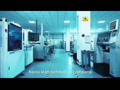
Workshop
Testing service
1. Manual visual inspection of PCB board
2. PCB board online test
3. PCB board function test
4. AOI (Automatic optical inspection)
5. Automatic X-ray inspection
6. Laser detection system
7. Size detection
Above is the PCB testing service.
Usually Haina lean Electronics Co.,Ltd PCBA Tech offers a full
range of testing service. Including:
1. AOI(Automatic Optical Inspection)
2. Function Testing
3. In Circuit Testing
4. Testing Jig
5. Testing Service
6. X-Ray for BGA Testing
7. Printing Solder Paste Test
Each board is carefully examined by our dedicated inspection team
using AOI and high magnification viewers.
Using our X-Ray machine, we test PCBs to component level and all
wiring is fully inspected and tested.
Flash testing and earth bonding tests can also be undertaken where
required.
Partners
Common packaging
PCB: Vacuum packaging with carton box
PCBA: ESD packaging with carton box
Why choose us?
Welcome to visit our factory, Haina lean Electronics Co., Ltd.
1. Experienced: Focus on PCB And PCBA munufacturing over 10 years.
2. Professional: Expertise engineer with barrier-free English
3. Rapid delivery: On-time delivery rate reaches 98%
4.Cost effective: No excessive profits. Lower cost with same
quality And service
FAQ
Q1.
What's your MOQ ?
No Moq ,We accept small orders as well as mass production.
Q2.
For small quantity orders, can you produce prototype PCB?
Haina lean Electronics Co., has the capability to produce circuit
boards in any amount.
Q3.
Can You provide fast rotating PCB ?
Yes , we can provide fast service 24 hours .
Q4.
What are the services you can provide ?
One-stop contract manufacturing
PCB board, PCB Design & Layout, PCB Assembly, PCBA programming &
functional testing, Electronic components purchasing service,
Enclosure molding & final assembly with
labels,instructions,enclosure, boxes.
Q5.
Whether all PCBA s will be tested before delivery ?
Yes , we will test each piece of PCBA product under your testing
methods ,to ensure quality and functionality .
Q6.
Do you provide OEM service ?
Yes ,we offer PCB and PCBA OEM Service , we manufacture the PCB and
PCBA products to your design and requirements .
Q7.
Shipping Cost ?
The shipping cost is determined by the destination ,weight ,packing
size of the goods .We can provide shipping, air, land, express and
other transportation services .
Q8.
Do you accept process materials supplied by clients?
Yes, we can provide component source, and we also accept component
from client. OEM and ODM orders are accepted.
Market Success:
Products are mainly exported to Europe and USA;
Our customers spread over more than 80 countries;
Products are widely used in various industries.
Company Information
Beijing Haina lean Electronics Co.,Ltd is one of the most professional PCB manufacture in Beijing,China. With more then 10 years of development, Haina Lean Electronics turns into a first class manufacture of HDI PCB ,with production capability 4000 square meters.
Our factory is providing high quality bare PCB, PCB layout design service and PCB assembly service,including components sourcing, function test,conformal coating and complete assembly for clients all.
We have profuse experience in manufacturing PCB,owned experienced technical R & D technology team, young and professional sales and customer service team, experienced and professional procurement team and assembly testing team, which make sure the products quality of the pass rate, on-time delivery rate of customer orders.
Our services include: circuit board design and layout, 2-46 layers PCB manufacturing, professional FPC production, electronic components purchasing, SMT professional processing, Soldering and Assembly, especially sample and small bulk orders. we have the advantages of a quick quote, fast production, fast delivery.
The company pursues "inclusiveness, excellence, people-oriented".
Constantly innovate, take technology as the core, regard quality as
life, and wholeheartedly provide customers with high-quality and
high-efficiency humanized services.We are willing to serve our
customers with the principle of continuous honesty &
trustworthiness, pragmatism and innovation.


One Stop PCB Assembly 6oz Tg170 Rigid Flex PCB Board
Inquiry Cart
0