
Add to Cart
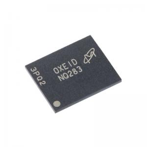
MT29F2G08ABAEAH4-IT:E NAND Flash Asynchronous SLC 2Gbit 8bit 35mA 256MX8 VFBGA-63
Specifications
| Product Attribute | Attribute Value |
|---|---|
| SMD/SMT | |
| 2 Gbit | |
| 256 M x 8 | |
| FBGA Code | NQ283 |
| 8 bit | |
| 2.7 V | |
| 3.6 V | |
| 35 mA | |
| - 40 C | |
| + 85 C |
Description
Micron NAND Flash devices include an asynchronous data interface for high-perform-ance I/O operations. These devices use a highly multiplexed 8-bit bus (I/Ox) to transfer commands, address, and data. There are five control signals used to implement the asynchronous data interface: CE#, CLE, ALE, WE#, and RE#. Additional signals control hardware write protection and monitor device status (R/B#).
This hardware interface creates a low pin-count device with a standard pinout that re-mains the same from one density to another, enabling future upgrades to higher densi-ties with no board redesign.
A target is the unit of memory accessed by a chip enable signal. A target contains one or more NAND Flash die. A NAND Flash die is the minimum unit that can independently execute commands and report status. A NAND Flash die, in the ONFI specification, is referred to as a logical unit (LUN). There is at least one NAND Flash die per chip enable signal. For further details, see Device and Array Organization.
This device has an internal 4-bit ECC that can be enabled using the GET/SET features. See Internal ECC and Spare Area Mapping for ECC for more information.
Array Addressing – MT29F2G08 (x8)
Notes: 1. Block address concatenated with page address = actual page address. CAx = column ad-dress; PAx = page address; BAx = block address.
2. If CA11 is 1, then CA[10:6] must be 0.
3. BA6 controls plane selection.
Features
• Open NAND Flash Interface (ONFI) 1.0-compliant1
• Single-level cell (SLC) technology
• Organization
– Page size x8: 2112 bytes (2048 + 64 bytes)
– Page size x16: 1056 words (1024 + 32 words)
– Block size: 64 pages (128K + 4K bytes)
– Plane size: 2 planes x 1024 blocks per plane
– Device size: 2Gb: 2048 blocks
• Asynchronous I/O performance – tRC/tWC: 20ns (3.3V), 25ns (1.8V)
• Array performance
– Read page: 25µs 3
– Program page: 200µs (TYP: 1.8V, 3.3V)3
– Erase block: 700µs (TYP)
• Command set: ONFI NAND Flash Protocol
• Advanced command set
– Program page cache mode4
– Read page cache mode 4
– One-time programmable (OTP) mode
– Two-plane commands 4
– Interleaved die (LUN) operations
– Read unique ID
– Block lock (1.8V only)
– Internal data move
• Operation status byte provides software method for detecting
– Operation completion
– Pass/fail condition
– Write-protect status
• Ready/Busy# (R/B#) signal provides a hardware method of detecting operation completion
• WP# signal: Write protect entire devic
• First block (block address 00h) is valid when ship-ped from factory with ECC. For minimum required ECC, see Error Management.
• Block 0 requires 1-bit ECC if PROGRAM/ERASE cycles are less than 1000
• RESET (FFh) required as first command after power-on
• Alternate method of device initialization (Nand_Init) after power up (contact factory)
• Internal data move operations supported within the plane from which data is read
• Quality and reliability
– Data retention: 10 years
– Endurance: 100,000 PROGRAM/ERASE cycles
• Operating voltage range
– VCC: 2.7–3.6V
– VCC: 1.7–1.95V
• Operating temperature
– Commercial: 0°C to +70°C – Industrial (IT): –40ºC to +85ºC
– Automotive Industrial (AIT): –40°C to +85°C
– Automotive (AAT): –40°C to +105°C
• Package – 48-pin TSOP type 1, CPL2 – 63-ball VFBGA
Trading Guides
| Shipping | Delivery period | For in-stock parts, orders are estimated to ship out in 3 days. |
| Shipping rates | After confirming the order, we will evaluate the shipping cost based on the weight of the goods | |
| Shipping option | We provide DHL, FedEx, EMS, SF Express, and Registered Air Mail international shipping. | |
| Shipping tracking | We will notify you by email with tracking number once order is shipped. | |
Returning warranty | Returning | Returns are normally accepted when completed within 30 days from date of shipment.Parts should be unused and in original packaging.Customer has to take charge for the shipping. |
| Warranty | All Retechip purchases come with a 30-day money-back return policy, This warranty shall not apply to any item where defects have been caused by improper customer assembly, failure by customer to follow instructions, product modification, negligent or improper operation | |
| Ordering | Payment | T/T,PayPal, Credit Card includes Visa, Master, American Express. |
