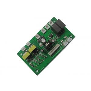
Mobile Amplifier Pcb Board Manufacturing Process Custom OEM PCB
Add to Cart

Oem Pcba/Quick Turn Pcb/Fr-4/Pcba/OEM Of Circuit Board
The wiring material is copper foil. Originally, the copper foil is covered on the whole board, but in the manufacturing process, the middle part is etched away, and the remaining part becomes a network of small lines. These lines are called conductors
pattern) or wiring, and used to provide circuit connection of parts on PCB. The PCB board is V-CUT
PCB, that is, there are several boards in a board, not a single out. Plate shipment is roughly the same, mold out of the plate when a four, six, eight and so on. Not single out to facilitate the production of SMD components.
Double-sided PCB board is a very important PCB board in the circuit board, the market has double-sided circuit board metal base PCB board, Hi-Tg heavy copper foil circuit board, flat winding double-sided circuit board, high frequency PCB, mixed dielectric base high frequency double-sided circuit board, etc. It is suitable for a wide range of high-tech industries such as: telecommunications, power supply, computer, industrial control, digital products, scientific and educational instruments, medical instruments, automobiles, aerospace defense and so on.
| Copper Thickness | 1oz~3oz,0.5-5 Oz | Base Material | FR4, Aluminium, TG, Rogers, CEM-1 |
| Board Thickness | 1.6mm, 0.5~3.2mm, 0.2-3.0mm, 0.3~2.5mm, 2.0mm | Min. Line Width | 3mi, 4mil, 0.1mm, 0.1mm(Flash Gold)/0.15mm(HASL), 0.1 0mm |
| Min. Hole Size | 0.25mm, 0.1mm, 0.2 Mm, 0.15-0.2mm, 0.1mm-1mm | Surface Finishing | HASL, OSP, ENIG, HASL Lead Free, Immersion Gold |
| Min. Line Spacing | 0.003", 4mil, 0.2mm, 0.15mm, 0.1mm4mil) | Product Name | Printed Circuit Board, 94V0 PCB Design / PCB Manufacturing |
| Application | Electronics Device, Consumer Electronics, Electronical Products, Industrial, And So On | Solder Mask | Blue, Green. Red. Blue. White. Black.Yellow, Green/black/white/red/blue Etc., |
| Layer | 1~20 Layers, 1-24layers | Rohs | Lead free |
What we need:
* Gerber files of the bare PCB
* Bill of materials to include: Manufacturer's part number, type of
part, type of packaging,
component locations listed by reference designators and quantity
* Dimensional specifications for non-standard components
* Assembly drawing, including any change notices
* Final test procedures (if available)
| Turnkey PCBA | PCB+components sourcing+assembly+package | ||||
| Assembly details | SMT and Thru-hole, ISO lines | ||||
| Lead Time | Prototype: 15 work days. Mass order: 20~25 work days | ||||
| Testing on products | Flying Probe Test, X-ray Inspection, AOI Test, functional test | ||||
| Quantity | Min quantity: 1pcs. Prototype, small order, mass order, all OK | ||||
| Files we need | PCB: Gerber files(CAM, PCB, PCBDOC) | ||||
| Files we need | Components: Bill of Materials(BOM list) | ||||
| Files we need | Assembly: Pick-N-Place file | ||||
| PCB panel Size | Min size: 0.25*0.25 inches(6*6mm) | ||||
| Max size: 20*20 inches(500*500mm) | |||||
| PCB Solder Type | Water Soluble Solder Paste, RoHS lead free | ||||
| Components details | Passive Down to 0201 size | ||||
| Components details | BGA and VFBGA | ||||
| Components details | Leadless Chip Carriers/CSP | ||||
| Components details | Double-sided SMT Assembly | ||||
| Components details | Fine Pitch to 0.8mils | ||||
| Components details | BGA Repair and Reball | ||||
| Components details | Part Removal and Replacement | ||||
| Component package | Cut Tape,Tube,Reels,Loose Parts | ||||
| PCB assembly | Drilling-----Exposure-----Plating-----Etaching & Stripping-----Punching-----Electrical Testing-----SMT-----Wave Soldering-----Assembling-----ICT-----Function Testing-----Temperature & Humidity Testing | ||||
Q: What files do you use in PCBA fabrication?
A: Gerber or Eagle, BOM listing, PNP and Components Position.
Q: Is it possible you could offer sample?
A: Yes, we can custom samples for your testing before mass production.
Q: How much time could I get the quotation after sent Gerber, BOM and test procedure?
A: Within 6 hours for PCB quotation and around 24 hours for PCBA quotation.
Q: How can I know the process of my PCBA production?
A: 7-10 days for PCB production and components purchasing, and 10 days for PCB assembly and Testing.
Q. Are my design secure when I send them to you?
Your files are held in complete safety and security while Kerongda is in possession of them.Your files are never shared with any third parties,only our colleagues have access to your design files.Since they are your property,we respect the copyright of your files.The customer controls the disposition of these files per your requirements and written approval.
Q.What is the warranty?
The warranty is 2years.


