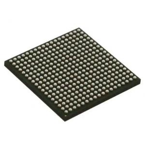
AM3357BZCZA30 IC Chip Mpu Sitara 300MHZ 324 NFBGA ADE Chip
Brand Name:original
Certification:original
Model Number:AM3357BZCZA30
Minimum Order Quantity:1
Delivery Time:1-3working days
Payment Terms:T/T, L/C
Contact Now
Add to Cart
Verified Supplier
Location:
Shenzhen Guangdong China
Address:
Room 405, Building A2, Niushang Zhigu, United Industrial Park, Fengtang Avenue, Shenzhen,Guangdong, China. Post code: 518100
Supplier`s last login times:
within 37 hours
Shipping
lt's easy to get a shipping quote! Just click the button below and complete the short form.
Get Shipping Quote
Product Details
Company Profile
Product Details
AM3357BZCZA30 Integrated Circuit IC Chip Mpu Sitara 300mhz 324nfbga
ARM® Cortex®-A8 Microprocessor IC Sitara™ 1 Core, 32-Bit 300MHz 324-NFBGA (15x15)
Specifications of AM3357BZCZA30
| TYPE | DESCRIPTION |
| Category | Integrated Circuits (ICs) |
| Embedded | |
| Microprocessors | |
| Mfr | Texas Instruments |
| Series | Sitara™ |
| Package | Tray |
| Product Status | Active |
| Core Processor | ARM® Cortex®-A8 |
| Number of Cores/Bus Width | 1 Core, 32-Bit |
| Speed | 300MHz |
| Co-Processors/DSP | Multimedia; NEON™ SIMD |
| RAM Controllers | LPDDR, DDR2, DDR3, DDR3L |
| Graphics Acceleration | Yes |
| Display & Interface Controllers | LCD, Touchscreen |
| Ethernet | 10/100/1000Mbps (2) |
| SATA | - |
| USB | USB 2.0 + PHY (2) |
| Voltage - I/O | 1.8V, 3.3V |
| Operating Temperature | -40°C ~ 105°C (TJ) |
| Security Features | Cryptography, Random Number Generator |
| Mounting Type | Surface Mount |
| Package / Case | 324-LFBGA |
| Supplier Device Package | 324-NFBGA (15x15) |
| Additional Interfaces | CAN, I²C, McASP, McSPI, MMC/SD/SDIO, UART |
| Base Product Number | AM3357 |
Features of AM3357BZCZA30
• Up to 1-GHz Sitara™ ARM® Cortex®
-A8 32‑BitRISC Processor
– NEON™ SIMD Coprocessor
– 32KB of L1 Instruction and 32KB of Data CacheWith Single-Error Detection (Parity)
– 256KB of L2 Cache With Error Correcting Code(ECC)
– 176KB of On-Chip Boot ROM
– 64KB of Dedicated RAM
– Emulation and Debug - JTAG
– Interrupt Controller (up to 128 InterruptRequests)
• On-Chip Memory (Shared L3 RAM)
– 64KB of General-Purpose On-Chip MemoryController (OCMC) RAM
– Accessible to All Masters
– Supports Retention for Fast Wakeup
• External Memory Interfaces (EMIF)
– mDDR(LPDDR), DDR2, DDR3, DDR3LController:
– mDDR: 200-MHz Clock (400-MHz Data Rate)
– DDR2: 266-MHz Clock (532-MHz Data Rate)
– DDR3: 400-MHz Clock (800-MHz Data Rate)
– DDR3L: 400-MHz Clock (800-MHz DataRate)
– 16-Bit Data Bus
– 1GB of Total Addressable Space
– Supports One x16 or Two x8 Memory DeviceConfigurations
– General-Purpose Memory Controller (GPMC)
– Flexible 8-Bit and 16-Bit AsynchronousMemory Interface With up to Seven ChipSelects (NAND, NOR, Muxed-NOR, SRAM)
– Uses BCH Code to Support 4-, 8-, or 16-BitECC
– Uses Hamming Code to Support 1-Bit ECC
– Error Locator Module (ELM)
– Used in Conjunction With the GPMC toLocate Addresses of Data Errors fromSyndrome Polynomials Generated Using aBCH Algorithm
– Supports 4-, 8-, and 16-Bit per 512-ByteBlock Error Location Based on BCHAlgorithms
• Programmable Real-Time Unit Subsystem andIndustrial Communication Subsystem (PRU-ICSS)
– Supports Protocols such as EtherCAT®,PROFIBUS, PROFINET, EtherNet/IP™, and More
– Two Programmable Real-Time Units (PRUs)
– 32-Bit Load/Store RISC Processor Capable of Running at 200 MHz
– 8KB of Instruction RAM With Single-Error Detection (Parity)
– 8KB of Data RAM With Single-Error Detection (Parity)
– Single-Cycle 32-Bit Multiplier With 64-Bit Accumulator
– Enhanced GPIO Module Provides ShiftIn/Out Support and Parallel
Latch on External Signal
– 12KB of Shared RAM With Single-Error Detection (Parity)
– Three 120-Byte Register Banks Accessible by Each PRU
– Interrupt Controller (INTC) for Handling System Input Events
– Local Interconnect Bus for Connecting Internal and External
Masters to the Resources Inside the PRU-ICSS
– Peripherals Inside the PRU-ICSS:
– One UART Port With Flow Control Pins, Supports up to 12 Mbps
– One Enhanced Capture (eCAP) Module
– Two MII Ethernet Ports that Support Industrial Ethernet, such as
EtherCAT
– One MDIO Port
• Power, Reset, and Clock Management (PRCM) Module
– Controls the Entry and Exit of Stand-By and Deep-Sleep Modes
– Responsible for Sleep Sequencing, Power Domain Switch-Off
Sequencing, Wake-Up Sequencing, and Power Domain Switch-On
Sequencing
– Clocks
– Integrated 15- to 35-MHz High-Frequency Oscillator Used to
Generate a Reference Clock for Various System and Peripheral Clocks
– Supports Individual Clock Enable and Disable Control for
Subsystems and Peripherals to Facilitate Reduced Power Consumption
– Five ADPLLs to Generate System Clocks
(MPU Subsystem, DDR Interface, USB and Peripherals [MMC and SD,
UART, SPI, I 2C], L3, L4, Ethernet, GFX [SGX530], LCD Pixel Clock)
Applications of AM3357BZCZA30
• Gaming Peripherals
• Home and Industrial Automation
• Consumer Medical Appliances
• Printers
• Smart Toll Systems
• Connected Vending Machines
• Weighing Scales
• Educational Consoles
• Advanced Toys
Environmental & Export Classifications of AM3357BZCZA30
| ATTRIBUTE | DESCRIPTION |
| RoHS Status | ROHS3 Compliant |
| Moisture Sensitivity Level (MSL) | 3 (168 Hours) |
| REACH Status | REACH Unaffected |
| ECCN | 5A992C |
| HTSUS | 8542.31.0001 |


AM3357BZCZA30 IC Chip Mpu Sitara 300MHZ 324 NFBGA ADE Chip
Inquiry Cart
0