
Add to Cart
Multi-Layer Printed Circuit Board Fabrication In Red/ Green Solder Mask High-Density Multi-Layer PCB Services
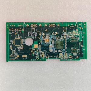
PCB Fabrication Description
PCB Fabrication is the process of preparing the bare board into a
certain form or structure according to the design documents and
specifications; And get them ready to assemble.As for the color of
the solder mask, we mainly provide green. In addition, we also
offer black, red and blue upon request.We provide multi-layer PCB
manufacturing and high-density multi-layer PCB services.
Once we have received all the details about the quote, we will review your quote, check the material availability, the complexity of the quote, the number of PCB factories, and then according to all requirements, we provide the customer with a lead time for PCB Fabrication
PCB Assembly Technical Capabilities
| Article | Description | Capability | |
| Sercive | PCB and SMT assembly with one-stop service | ||
| Files we need | PCB: Gerber files(CAM, PCB, PCBDOC) | ||
| Components: Bill of Materials(BOM list) | |||
| Assembly: Pick-N-Place file | |||
| Material | Laminate materials | FR4, high TG FR4, high frequency, alum, FPC | |
| Board cutting | Number of layers | 1-32 | |
| Min.thickness for inner layers | 0.003”(0.07mm) | ||
| (Cu thickness are excluded) | |||
| Board thickness | Standard | (0.1-4mm±10%) | |
| Min. | Single/Double:0.008±0.004” | ||
| 4layer:0.01±0.008” | |||
| 8layer:0.01±0.008” | |||
| Bow and twist | 7/1000 | ||
| Copper weight | Outer Cu weight | 0.5-4 0z | |
| Inner Cu weight | 0.5-3 0z | ||
| Drilling | Min size | 0.0078”(0.2mm) | |
| Drill deviation | ±0.002″(0.05mm) | ||
| PTH hole tolerance | ±0.002″(0.005mm) | ||
| NPTH hole tolerance | ±0.002″(0.005mm) | ||
| Solder mask | Color | Green,white,black,red,blue… | |
| Min solder mask clearanace | 0.003″(0.07mm) | ||
| Thickness | (0.012*0.017mm) | ||
| Silkscreen | Color | white,black,yellow,blue… | |
| Min size | 0.006″(0.15mm) | ||
| E-test | Function Test | 100% Functional test | |
| PCBA Testing | X-ray,AOI Test,Functional test | ||
| Pcb assembly | one-stop service electronic manufacxturer service | ||
| Component sourcing | Yes | ||
| Certificate | IATF16949,ROHS,UL | ||
| Delivery time: | PCB | 3-12days | |
| PCBA | 8-20days | ||
| Tolerance of pcb | ±5% | ||
| Max size of finish board | 450*450mm | ||
| MOQ | NO MOQ (1pcs) | ||
| Surface Finish | HASL,ENIG,immersion silver,immersion tin,OSP… | ||
| PCB outline | Square,circle,irregular(with jigs) | ||
| package | QFN,BGA,SSOP,PLCC,LGA | ||
FAQ
1).Q: How to process it if i have no drawing?
A: Firstly let us know your detail requirements( if you have
sample, please ship to us, we will copy it). Secondly We quote
according to your requirements or our suggestions. Thirdly customer
confirms the samples and places deposit for formal order. Fourthly
We arrange the production.
2).Q: What is the MOQ and fastest deliver time?
A: 1 pcs prototype+air express like DHL/UPS/FedEx/TNT.
3).Q: What kind of files you need to PCBA quotations?
A: PCB files (Gerber), Bom list, XY Data (pick-N-place).
4).Q: Do you support OEM PCB services?
A: Yes, our R&D team is experienced and help you make your
ideas come ture.
5).Q: Is it OK to print my logo on product?
A: Yes. Please inform us formally before our production and confirm
the design firstly based on our sample.

