
Add to Cart
Double Sided FR4 CEM3 PCB Assembly Circuit Board Fabrication Assembly One Stop Service
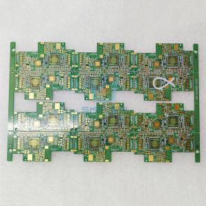
Double Sided Board Fabrication
Double Sided Board is a printed circuit board with copper on both
sides of Top (top layer) and Bottom (bottom layer), both sides can
be wired and welded, and the middle is a layer of insulation layer,
which is a commonly used printed circuit board. Both sides can be
wired, greatly reducing the difficulty of wiring, so it is widely
used.
Both sides of the Double Sided Board have wiring, but to use the
wires on both sides, there must be an appropriate circuit
connection between the two sides. This "bridge" between circuits is
called a pilot hole. A pilot hole is a small hole filled with or
coated with metal on the PCB board, which can be connected with
wires on both sides. Because the area of the Double Sided Board is
twice as large as that of the Single Sided Board, the Double Sided
Board solves the difficulty of the Single Sided Board because of
the wiring interleaving (which can be channeled through the hole to
the other side), and it is more suitable for more complex circuits
than the Single Sided Board.
Shenzhen Sky-Win is a one-stop PCBA service provider - Our current focus on the PCBA one-stop supplier schematic design, software development, PCB Layout, a full set of material purchasing, SMT+DIP manufacturing, board direct supply and other OEM/ODM services.
PCB Assembly Technical Capabilities
| Article | Description | Capability | |
| Sercive | PCB and SMT assembly with one-stop service | ||
| Files we need | PCB: Gerber files(CAM, PCB, PCBDOC) | ||
| Components: Bill of Materials(BOM list) | |||
| Assembly: Pick-N-Place file | |||
| Material | Laminate materials | FR4, high TG FR4, high frequency, alum, FPC | |
| Board cutting | Number of layers | 1-32 | |
| Min.thickness for inner layers | 0.003”(0.07mm) | ||
| (Cu thickness are excluded) | |||
| Board thickness | Standard | (0.1-4mm±10%) | |
| Min. | Single/Double:0.008±0.004” | ||
| 4layer:0.01±0.008” | |||
| 8layer:0.01±0.008” | |||
| Bow and twist | 7/1000 | ||
| Copper weight | Outer Cu weight | 0.5-4 0z | |
| Inner Cu weight | 0.5-3 0z | ||
| Drilling | Min size | 0.0078”(0.2mm) | |
| Drill deviation | ±0.002″(0.05mm) | ||
| PTH hole tolerance | ±0.002″(0.005mm) | ||
| NPTH hole tolerance | ±0.002″(0.005mm) | ||
| Solder mask | Color | Green,white,black,red,blue… | |
| Min solder mask clearanace | 0.003″(0.07mm) | ||
| Thickness | (0.012*0.017mm) | ||
| Silkscreen | Color | white,black,yellow,blue… | |
| Min size | 0.006″(0.15mm) | ||
| E-test | Function Test | 100% Functional test | |
| PCBA Testing | X-ray,AOI Test,Functional test | ||
| Pcb assembly | one-stop service electronic manufacxturer service | ||
| Component sourcing | Yes | ||
| Certificate | IATF16949,ROHS,UL | ||
| Delivery time: | PCB | 3-12days | |
| PCBA | 8-20days | ||
| Tolerance of pcb | ±5% | ||
| Max size of finish board | 450*450mm | ||
| MOQ | NO MOQ (1pcs) | ||
| Surface Finish | HASL,ENIG,immersion silver,immersion tin,OSP… | ||
| PCB outline | Square,circle,irregular(with jigs) | ||
| package | QFN,BGA,SSOP,PLCC,LGA | ||
FAQ
1).Q: How to process it if i have no drawing?
A: Firstly let us know your detail requirements( if you have
sample, please ship to us, we will copy it). Secondly We quote
according to your requirements or our suggestions. Thirdly customer
confirms the samples and places deposit for formal order. Fourthly
We arrange the production.
2).Q: What is the MOQ and fastest deliver time?
A: 1 pcs prototype+air express like DHL/UPS/FedEx/TNT.
3).Q: What kind of files you need to PCBA quotations?
A: PCB files (Gerber), Bom list, XY Data (pick-N-place).
4).Q: Do you support OEM PCB services?
A: Yes, our R&D team is experienced and help you make your
ideas come ture.
5).Q: Is it OK to print my logo on product?
A: Yes. Please inform us formally before our production and confirm
the design firstly based on our sample.
