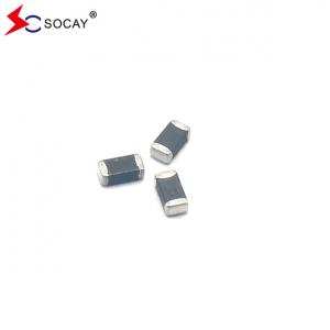
1206 Multilayer Chip Varistor SV1206N220G0A For Motherboard Notebook
Brand Name:SOCAY
Certification:REACH RoHS ISO
Model Number:SV1206N220G0A
Minimum Order Quantity:3000PCS
Delivery Time:5-8 work days
Place of Origin:Shenzhen Guangdong China
Contact Now
Add to Cart
Verified Supplier
Location:
Shenzhen Guangdong China
Address:
4/F, Block C, HeHengXing Science & Technology Park, 19 MinQing Road, LongHua District, Shenzhen City, GuangDong Province, China
Supplier`s last login times:
within 40 hours
Shipping
lt's easy to get a shipping quote! Just click the button below and complete the short form.
Get Shipping Quote
Product Details
Company Profile
Product Details
1206 Multilayer Chip Varistor SV1206N220G0A Application for Mother Board, Notebook
Multilayer Chip Varistor DATASHEET: SV1206N220G0A_v209.1.pdf
Description:
The Multilayer Chip Varistor SV1206N220G0A is based on Multilayer
fabrication technology. These components are designed to suppress a
variety of transient events, including those specified in IEC
61000-4-2 or other standards used for Electromagnetic Compliance
(EMC). The SV1206N220G0A is typically applied to protect integrated
circuits and other components at the circuit board level. It can
operate over a wider temperature range than zener diodes.
Multilayer Chip Varistor Electrical Characteristics (25±5℃):
| Symbol | Minimum | Typical | Maximum | Units |
| VRMS | — | — | 17 | V |
| VDC | — | — | 22 | V |
| VV | 26.4 | — | 33 | V |
| VC | — | — | 72 | V |
| Imax | — | — | 100 | A |
| Wmax | — | — | 0.5 | W |
VRMS - Maximum AC operating voltage the varistor can maintain and not exceed 10μA leakage current.
VDC - Maximum DC operating voltage the varistor can maintain and not exceed 10μA leakage current.
VV - Voltage across the device measure at 1mA DC current.
Equivalent to VB “breakdown voltage”.
VC - Maximum peak current across the varistor with 8/20μs waveform and 5A pulse current.
Imax - Maximum peak current which may be applied with 8/20μs waveform without device failure.
Wmax - Maximum energy which may be dissipated with the 10/1000μs waveform without device failure.
Multilayer Chip Varistor Features:
|
Multilayer Chip Varistor Applications:
|
Multilayer Chip Varistor Construction & Dimensions:
| Size EIA (EIAJ) | Length (L) | Width (W) | Thickness (T) | |||
| Inches | Millimeters | Inches | Millimeters | Inches | Millimeters | |
| 1206 (3216) | 0.126±0.012 | 3.20±0.30 | 0.063±0.012 | 1.60±0.30 | 0.071 Max | 1.80 Max |
Multilayer Chip Varistor IR Soldering:
| Rapid heating, partial heating or rapid cooling will easily cause defect of the component. So preheating and gradual cooling process is suggested. IR soldering has the highest yields due to controlled heating rates and solder liquidus times. Make sure that the element is not subjected to a thermal gradient steeper than 4 degrees per second. 2 degrees per second is the ideal gradient. During the soldering process, pre-heating to within 100 degrees of the solder peak temperature is essential to minimize thermal shock. |
Soldering Recommendations:
|
Multilayer Chip Varistor Environmental & Reliability Testing:
| Characteristic | Test method and description | |||
| High Temperature Storage | The specimen shall be subjected to125±2℃ for 1000±2 hours in a thermostatic bath without load and then stored at room temperature and humidity for 1 to 2 hours. The change of varistor voltage shall be within 10%. | |||
| Temperature Cycle | The temperature cycle of specified temperature shall be repeated five times and then stored at room temperature and humidity for one two hours. The change of varistor voltage shall be within 10% and mechanical damage shall be examined. | Step | Temperture | Period |
| 1 | -40±3℃ | 30min±3 | ||
| 2 | Room Temperature | 1~2hours | ||
| 3 | 125±2℃ | 30min±3 | ||
| 4 | Room Temperature | 1~2hours | ||
| High Temperature Load | After being continuously applied the maximum allowable voltage at 85℃ for 1000hours, the specimen shall be stored at room temperature and humidity for one or hours, the change of varistor voltage shall be within 10%. | |||
Damp Heat Load/ Humidity Load | The specimen should be subjected to 40℃,90 to 95%RH environment, and the maximum allowable voltage applied for 1000 hours, then stored at room temperature and humidity for one or two hours. The change of varistor voltage shall be within 10%. | |||
| Low Temperature Storage | The specimen should be subjected to -40℃, without load for 1000 hours and then stored at room temperature for one two hours. The change of varistor voltage shall be within 10%. | |||
Quantity of Products in The Taping Package:
| SIZE EIA (EIAJ) | 1206 (3216) |
| Standard Packing Quantity (PCS / reel) | 3,000 |


1206 Multilayer Chip Varistor SV1206N220G0A For Motherboard Notebook
Inquiry Cart
0