High Density Interconnect High Layer PCB 0.1mm Min Solder Mask Clearance
Brand Name:Ben Qiang
Certification:ISO/TS16949/RoHS/TS16949
Model Number:FR-4/Rogers
Minimum Order Quantity:1PCS
Delivery Time:3-7 days delivery
Payment Terms:Bank Transfer/Alipay/PayPal
Contact Now
Add to Cart
Verified Supplier
Location:
Shenzhen China
Address:
Building C5/B6, Yanchuan North Industrial Park, Yanluo Street, Baoan District, Shenzhen, China
Supplier`s last login times:
within 12 hours
Shipping
lt's easy to get a shipping quote! Just click the button below and complete the short form.
Get Shipping Quote
Product Details
Company Profile
Product Details
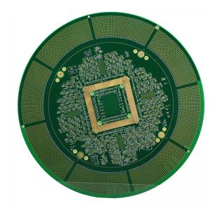
High Layer PCB Board with 0.1mm Min. Solder Mask Clearance for High Layer Design
Product Description:
Features:
- Product Name: High Layer PCB
- Layer Count: High Layer
- Solder Mask Color: Green, Blue, Black, Red, Yellow, White
- Impedance Control: Yes
- Min. Line Width/Spacing: 3mil/3mil
- Copper Thickness: 1/3 Oz To 2 Oz
- Key Features:
- High Density Interconnect PCB
- High Layer Printed Circuit Board
- High Layer PCB Board
- HDI PCB
Technical Parameters:
Applications:
High Layer PCB - A High Density Interconnect Solution for Complex
Circuits
High Layer PCB, also known as High Layer Multilayer Board, is a type of printed circuit board (PCB) that is designed for complex circuits with multiple layers of conductive material. This advanced PCB technology is widely used in various applications, including consumer electronics, medical devices, industrial equipment, and more.
With a High Layer PCB, you can achieve higher circuit density, better signal integrity, and improved thermal management for your electronic devices. This makes it an ideal choice for high-performance applications that require efficient and reliable operation.
Product Attributes
- Lead Time: 3-5 Days
- Silkscreen Color: White, Black, Yellow
- Layer Count: High Layer
- Surface Finish: HASL, ENIG, OSP, Immersion Silver, Immersion Tin
- Board Thickness: 0.2mm To 6.0mm
Application Scenarios
High Layer PCBs are particularly useful in applications that require complex circuits with high-density interconnects. Some of the common application scenarios for this type of PCB include:
- Consumer Electronics: High Layer PCBs are widely used in consumer electronics such as smartphones, laptops, and tablets, where space is limited and complex circuits need to be packed into a compact design.
- Medical Devices: In medical devices, High Layer PCBs are used to create sophisticated circuits that can perform precise and accurate operations. This is essential for devices such as MRI machines, pacemakers, and ultrasound equipment.
- Industrial Equipment: Industrial equipment, such as robots, automation systems, and control panels, require complex circuits with high-density interconnects for efficient and reliable operation. High Layer PCBs are an ideal choice for such applications.
High Layer PCB Prototype
High Layer PCBs can be prototyped to test the functionality and performance of the circuit before mass production. This is particularly beneficial in applications where the circuit design is complex and requires multiple iterations for optimization. The High Layer PCB prototype allows engineers to identify any design flaws and make necessary changes before the final product is manufactured. This reduces the risk of costly errors and ensures the final product meets the desired specifications.
Overall, High Layer PCBs offer a reliable and efficient solution for complex circuits with high-density interconnects. With a quick lead time, a variety of silkscreen color options, and a range of surface finishes to choose from, High Layer PCBs are a versatile and in-demand product for various industries.
Customization:
Customized Services for High Layer PCB
We offer customizable solutions for High Layer PCB, also known as High Density Interconnect Board or High Density Interconnect PCB, to meet your specific requirements and deliver superior performance. Our services are designed to provide you with the highest quality and reliability in the industry.
- Min. Line Width/Spacing: 3mil/3mil
- Rohs Compliant: Yes
- Lead Time: 3-5 Days
- Surface Finish: HASL, ENIG, OSP, Immersion Silver, Immersion Tin
- Material: FR-4
Our skilled team of experts uses the latest technology and techniques to ensure that your High Layer PCB meets your exact specifications. We understand the importance of precision and accuracy in High Density Interconnect Boards, and we are committed to delivering the best results for your project.
With our customizable services, you have the flexibility to choose the materials, surface finishes, and lead time that best suit your needs. Our efficient processes and state-of-the-art equipment enable us to deliver your custom High Layer PCB on time and with the highest quality.
Invest in our customized services for High Layer PCB and experience the difference in performance and reliability. Contact us to discuss your project and receive a quote today.
Packing and Shipping:
High Layer PCB Packaging and Shipping
High Layer PCBs are carefully packaged and shipped to ensure safe delivery to customers. Our packaging process follows industry standards and best practices to protect the delicate circuit boards during transportation.
Each High Layer PCB is first wrapped in anti-static foam to prevent electrostatic discharge and damage to the components. It is then placed in a sturdy cardboard box with additional padding for shock absorption. The box is sealed with high-quality packaging tape to ensure the PCB stays secure during transit.
For international shipments, we use custom-made wooden crates to provide extra protection and stability. The crates are designed to withstand rough handling and extreme weather conditions, ensuring the PCBs arrive in perfect condition.
Our shipping partners are carefully selected for their reliability and efficiency in delivering packages. We offer a variety of shipping options to meet our customers' needs, including express delivery for urgent orders.
Upon shipment, customers will receive a tracking number to monitor the progress of their package. Our customer service team is also available to assist with any shipping inquiries or concerns.
We take great care in packaging and shipping our High Layer PCBs to ensure they reach our customers in pristine condition.
FAQ:
- Q: What is the main purpose of High Layer PCB?
- A: The main purpose of High Layer PCB is to provide a more compact and efficient circuit design for complex electronic devices.
- Q: What are some advantages of using High Layer PCB?
- A: Some advantages of using High Layer PCB include higher density of components, reduced size and weight of the device, and improved signal integrity.
- Q: How many layers does High Layer PCB typically have?
- A: High Layer PCB typically has 6 or more layers, but can go up to 50 layers or more for extremely complex designs.
- Q: What materials are used in High Layer PCB?
- A: High Layer PCB is typically made of fiberglass, copper, and various types of resins, such as epoxy or polyimide.
- Q: What types of electronic devices are High Layer PCB commonly used in?
- A: High Layer PCB is commonly used in smartphones, computers, medical devices, aerospace equipment, and other complex electronic devices.


High Density Interconnect High Layer PCB 0.1mm Min Solder Mask Clearance
Inquiry Cart
0