Product Details
CVD Electronic-Grade Diamond: Precision-Engineered Material
Synthesized via chemical vapor deposition, electronic-grade CVD
diamond achieves defect-free crystalline structures tailored for
advanced technical applications. Offering superior heat
dissipation, electrical insulation, and mechanical durability, this
material outperforms natural diamonds in controlled purity and
functional consistency.
Core Specifications
Dimensions: Customizable from 1×1 mm to 20×20 mm
Thickness Range: 0.3 mm – 3 mm
Surface Options:
Edge Configurations: Laser-cut precision or polished finishes
Industry Applications
Quantum Systems: Utilizes NV center defects for quantum computing qubits and
ultra-sensitive detectors.
Thermal Solutions: Manages extreme heat in high-frequency lasers and power
semiconductors.
Medical Precision: Enhances surgical scalpels and radiation monitoring devices with
biocompatible surfaces.
Optical Durability: Deploys in abrasive-resistant lenses for aerospace and industrial
imaging systems.
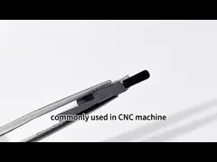
Tooling Excellence: Extends operational life in diamond-coated drills and cutting
blades.
Performance Classification
Electronics Tier: Quantum optics, particle detection
Optical Tier: Sensor windows, pressure anvils
Industrial Tier: Wear-resistant machining tools
Summary: As a transformative synthetic material, electronic-grade CVD
diamond enables advancements in quantum research, medical
instrumentation, industrial engineering, and optical technologies.
Size Available:
Crystal growth process: | Mono crystal CVD diamond |
Color: | Normal grade - Near colorless, Mechanic grade - Brown |
| 1) Regular shape, uniform size. The size can be strictly controlled
according to customer needs. |
2) High repurchase rate and high cost performance, well received by
customers. |
3) No visible growth lines,under 100x microscope, no black spots,
no impurities, no crack. |
4) The stress is good, the number of times of reuse is high, and it
is not easy to crac |
Size | 7*7 8*8 9*9 10*10 11*11 12*12 13*13 14*14 Thickness: 0.05-3mm |
Orientation: | 4pt/100 |
Shape: | Square,Triangles, rectangles, swords |
Lateral Dimensions Measured | to smaller side |
Edges | Laser Cut |
Laser Kerf | < 3° |
Lateral Tolerance: | +0.1/-0 mm |
Roughness, Ra | 1. Two sides polished, Ra <10- 30 nm |
| 2. One side polished, the other size is The other side is the
cutting surface, or grow |
| 3.Both sides are unpolished |
Summary: A multifunctional material, electronic-grade CVD diamond drives
innovation across quantum computing, medical devices, industrial
engineering, and high-performance optics.
Picture details:
Company Profile
Shaper Diamond Technology Co., Ltd. was established in 2008 in
Zhuzhou City, Hunan Province, China. Since its inception, the
company has been dedicated to researching, developing, producing,
and selling HPHT synthetic diamond and superhard material products.
Over the years, Shaper Diamond has continuously invested in
technology and equipment, enabling the company to achieve leading
status in the industry.
Advantages:
- Strong technical force: Shaper Diamond has a professional team
composed of highly skilled technical experts. The company has also
independently developed a number of patents related to HPHT
synthetic diamond and superhard material production technology.
- Advanced equipment: Shaper Diamond has invested heavily in advanced
equipment and facilities to ensure high-quality production. The
company's equipment includes high-pressure and high-temperature
synthesis equipment, precision diamond sawing machines, and diamond
polishing machines.
- Strong product strength: Shaper Diamond's products have high wear
resistance, high hardness, low friction coefficient, and other
characteristics. The company's products are widely used in the
fields of machinery, tooling, mining, and other industries.
- Excellent reputation: Shaper Diamond has always adhered to the
concept of quality first and integrity-based business. The company
has won a good reputation from customers at home and abroad through
its excellent product quality and excellent after-sales service.
The products cover sawing grade diamond, abrasive grade diamond,
dressing and machining grade large single crystal diamond, and
gemstone grade diamond.