FR4 1.0mm Order Custom PCB Board For Automobile Amplifier Audio
Brand Name:HF
Certification:ISO CE
Model Number:PCB
Minimum Order Quantity:5PCS
Delivery Time:5~8 days
Payment Terms:L/C, T/T,PAYPAL
Contact Now
Add to Cart
Verified Supplier
Location:
Shenzhen China
Address:
First Floor, Building A, No. 207, Xingye 2nd Road, Baoan, Shenzhen City
Supplier`s last login times:
within 36 hours
Shipping
lt's easy to get a shipping quote! Just click the button below and complete the short form.
Get Shipping Quote
Product Details
Company Profile
Product Details
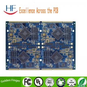
Audio Fr4 1.0mm Red PCB Automobile Power Amplifier Circuit Board
| High precision prototype | PCB bulk production | ||
| Max Layers | 4 layers | 8layers | |
| MIN Line width(mil) | 4mil | 4mil | |
| MIN Line space(mil) | 4mil | 4mil | |
| Min via (mechanical drilling) | Board thickness≤1.2mm | 0.05mm | 0.2mm |
| Board thickness≤2.5mm | 0.3mm | 0.3mm | |
| Board thickness>2.5mm | Aspect Ration≤13:1 | Aspect Ration≤13:1 | |
| Board thickness | MAX | 8mm | 7mm |
| MIN | 4 layers:0.35mm; | 2 layers:0.2mm; | |
| MAX Board size | 610*1200mm | 610*1200mm | |
| Max copper thickness | 4oz | 4oz | |
| Immersion Gold/ Gold Plated Thickness | Immersion Gold:Au,1—8u” Gold finger:Au,1—150u” Gold Plated:Au,1—150u” Nickel Plated :50—500u” | ||
| Hole copper thick | 25um 1mil | 25um 1mil | |
| Tolerance | Board thickness | Board thickness≤1.0mm:+/-0.1mm 1.0mm<Board thickness≤2.0mm:+/-10% Board thickness>2.0mm:+/-8% | Board thickness≤1.0mm:+/-0.1mm 1.0mm<Board thickness≤2.0mm:+/-10% Board thickness>2.0mm:+/-8% |
| Outline Tolerance | ≤100mm:+/-0.1mm 100< ≤300mm:+/-0.15mm >300mm:+/-0.2mm | ≤100mm:+/-0.13mm 100< ≤300mm:+/-0.15mm >300mm:+/-0.2mm | |
| Impedance | ±10% | ±10% | |
| MIN Solder mask bridge | 0.08mm | 0.10mm | |
| Plugging Vias capability | 0.35mm | 0.60mm | |
The basic design process of the circuit board can be divided into
the following four steps:
The design of circuit schematic diagram
The design of circuit schematic diagram is mainly the use of Protel
DXP schematic editor to draw schematic diagram.
⑵ Generate network reports
The network report is the report that shows the link relationship
between the circuit principle and the various components. It is the
bridge and link between the circuit schematic design and the
circuit board design (PCB design). Through the network report of
the circuit schematic diagram, it can quickly find the connection
between the components, so as to provide convenience for the later
PCB design.
⑶ Design of printed circuit board
The design of the printed circuit board is what we usually call the
PCB design, which is the final form of the conversion of the
circuit schematic diagram. The relevant design of this part is more
difficult than the design of the circuit schematic diagram. We can
complete the design of this part with the help of the powerful
design function of Protel DXP.
(4) Generate printed circuit board reports
After the printed circuit board design is completed, it is
necessary to generate various reports, such as generating pin
reports, circuit board information reports, network status reports,
etc., and finally print out the printed circuit diagram.
The design of the circuit schematic diagram is the foundation of
the whole circuit design. The quality of its design directly
determines the effect of PCB design.Generally speaking, the design
process of circuit schematic diagram can be divided into the
following seven steps:
⑴ Start Protel DXP schematic editor
Set the size and layout of the circuit schematic diagram
⑶ Remove the required components from the component library and
place them on the working plane
(4) Connect the components according to the design needs
⑸ Adjust the components after wiring
It saves the schematic diagram documents that have been drawn
⑺ prints out the drawing
The size, orientation, and color of the drawing are mainly realized
in the "Documents Options" dialog box. Press the Design→Options
command to open the "Documents Options" dialog box. In the Standard
Styles area, you can set the size of the drawing, click the button,
and select A4~ Orcade paper shapes in the drop-down list box.Set
the Orientation of the drawing through the Orientation option in
the Options section of the "Documents Options" dialog box. Click
the button, select Landscape, and set the horizontal drawing.Select
Portrait and set the vertical drawing.The setting of drawing Color
can be realized in the Options section of the drawing setting
dialog box. Click the Border Color block to set the drawing Border
Color, and click the Sheet Color block to set the drawing
background Color.
(4) Execution of the Design→Options→Change System Font command. The
"Font" dialog box pops up. Through the dialog box, the user can set
the System Font, the color, the size and the Font used in the
System Font.
The Settings of the grid and cursor are mainly implemented in the
"Preferences" dialog box. To open the "Preferences" dialog box,
execute the Tools→Preferences command.
Set Grid: Select the Graphical Editing TAB in the "Preferences"
dialog box that opens. In the Visible Grids column of the Ccursor
Grid Options section, select the Line Grid option for Setting
Linear Grid and the Dot Grid option for Point Grid (Grid-free).
Set Cursor: Select the Cursor Type option of Cursor Grid Options in
the Graphical Editing TAB. There are three Cursor types under this
option: Large Cursor90, Small Cursor90, and Small Cursor45. The
user can select any of the three Cursor types.
Plate-making technology
PCB board technology, including computer aided manufacturing
processing technology, namely CAD/CAM, and light painting
technology.The following is the introduction of computer aided
manufacturing processing technology
Computer-aided manufacturing (CAM) is the process of processing
according to the determined process.All the process requirements
mentioned in front of us should make the necessary preparations
before light painting.For example, mirroring, welding resistance
expansion, process line, process frame, line width adjustment,
center hole, contour line and other issues are to be in
CAM process to complete.In particular, small Spaces in user files
must be handled accordingly.Because the process flow and technical
level of each factory are different, in order to meet the final
requirements of users, necessary adjustments must be made in the
production process to meet the needs of users
The requirements of all aspects such as precision.Therefore, CAM
processing is an essential process in modern printed circuit
manufacturing.
What CAM has done
Correction of pad size. Combination of D code.
The correction of the line width, combined with D code.
The minimum spacing should be inspected, between pads and pads,
between pads and lines, and between lines.
4. Check the aperture size of the guest.
5. Check the minimum line width.
Pictures of welding to determine the expansion parameter.
7. Press Mirror.
8. Add various process lines and process boxes.
Its width is corrected to correct side erosion.
The adhesive will form the central hole.
Learn to add shape corner lines.
126. 126.
2, 2, 2, 2, 2, 2, 2, 2, 2, 3, 3, 3
⒕ spell.
⒖ graphic overlay processing, cutting Angle tangent handle.
Trademark ⒗ add users.
Organization of CAM process
As the popular CAD software on the market as many as dozens of, so
the management of the CAD process must first start from the
organization, good organization will achieve twice the result with
half the effort.
Since Gerber data format has become the standard in the light
painting industry, Gerber data should be taken as the processing
object in the whole light painting process.The following problems
arise if CAD data is used as an object.
1. There are too many kinds of CAD software. If all kinds of
process requirements are to be completed in the CAD software, it
requires every operator to be skilled in the operation of each CAD
software.This will require a long training period before the
operator can become a skilled worker to meet the actual production
requirements.
This is not economical in terms of time and economy.
2. Because of the many process requirements, some requirements for
some CAD software is impossible to achieve.Because the CAD software
is to do the design with, did not take into account the special
requirements in the process, so can not meet all the
requirements.The CAM software is specifically designed for
processing,
These jobs are at your best.
The CAM software was powerful, but all operations were performed on
Getber files, not CAD files.
If the CAD process is used, each operator is required to be
equipped with all the CAD software, and each CAD software has
different process requirements.This will create unnecessary
confusion for management.
To sum up, CAM organizations should be the following structures
(especially large and medium-sized enterprises).
(1) All process processing should take Gerber data as the
processing object.
Each operator must master the skill of converting CAD data into
Gerber data.
⑶ Each operator must master one or more operation methods of CAM
software.
(4) Establish a unified process specification for Gerber data
files.
CAM processes can be handled relatively centrally by several
operators for management purposes.Reasonable organization will
greatly improve the management efficiency, production efficiency,
and effectively reduce the error rate, so as to achieve the effect
of improving product quality.
FAQ
Q1: What service do you have?
A: We are the factory. We have our PCB manufacturing & Assembly factory.
We can offer a one-stop service from PCB manufacturing to PCB assembling, testing, housing, and other value-added services.
Q2. What is needed for PCB or PCBA quotation?
A: PCB: Quantity, Gerber file, and Technic requirements(material,
surface finish treatment, copper thickness, board thickness,...)
PCBA: PCB information, BOM, (Testing documents...)
Q3. What file formats do you accept for PCB and PCBA production?
A: Gerber file: CAM350 RS274X
PCB file: Protel 99SE, P-CAD 2001 PCB
BOM: Excel (PDF,word,txt)
Q4: What any other information should be offered except for the file?
A5: Following specifications are needed for the quotation:
a) Base material
b) Board thickness:
c) Copper thickness
d) Surface treatment:
e) color of solder mask and silkscreen
f) Quantity
Q5: What is your minimum order quantity?
A: Our MOQ is 1 PCS.
Q6. Shipping cost?
A: The shipping cost is determined by the destination, weight, packing size of the goods. Please let us know if you need us to quote you the shipping cost.
Q7: Are my PCB files safe when I submit them to you for manufacturing?
A: We respect customer's copyright and will never manufacture PCB for someone else with your files unless we receive written. Permission from you, nor we'll share these files with any other 3rd parties.
Q8: No PCB file/Gbr file, only have the PCB sample, can you produce it for me?
A: Yes, we could help you to clone the PCB. Just send the sample PCB to us, we could clone the PCB design and work out it.
Q9: What payment do you accept?
A:-Wire Transfer(T/T)
-Western Union
-Letter of Credit(L/C)
-Paypal
-Ali Pay
-Credit Card
We recommend bank transfer.
Q10: How to get the PCBs?
A: For small packages, we will ship the boards to you by DHL, UPS, FedEx, EMS. Door to door service! You will get your PCBs at your home.
For bulky goods more than 300kg, we may ship your PC boards by ship or by air to save freight costs. Of course, if you have your forwarder, we may contact them to deal with your shipment.
Q11. How about the delivery?
Usually, for sample order, our delivery is about five days. For small-batch, our delivery is about seven days.
For the mass production batch, our delivery is about ten days.
But that depends on the real condition when we get your order.
If your order is urgent, please contact us directly, we will make a priority to deal with it and do our best to give you a satisfied delivery time.
Q12: How about your factory production capacity?
A: we can provide 40000 square meter/month.
Q13: Which countries have you worked with?
A: US, Canada, Italy, Germany, Czech Republic, Australia, Japan, Spain, Portugal, France, Britain, Poland, Ukraine, Russia, Brazil, Argentina, and so on.
Q14: How do you ensure the final quality of the product
For PCB, we will use the Flying Probe Test, E-test, etc. for it.
For PCBA, we need you to offer us a method or test fixture for the function test. Before that, our inspectors will use a microscope and X-ray to check the IC foot welding or bad solder, etc.
Q15: Will you check my files before production?
A: Yes, our engineer will check your Gerber file and BOM list to avoid any mistake.
Q16: My budget is limited; can you provide solutions to save cost?
A: Yes, we can. For example, for PCBA: Replace the DIP components with SMD components, so it can narrow the PCB board size to save cost. Re-layout the PCB to reduce the size, it can save cost. Also, we can recommend alternative components.
Q17: Do you accept process materials supplied by clients?
A: Yes, we can provide the component source, and we also accept component from the client.
Q18: Can we visit your company?
No problem. You are welcome to visit us in Shenzhen.
Q19: I am delighted after I read your information, how can I start to purchase my order?
A: Fill in the form below and click the "send" button to send your order to us, or contact our sales on sales representative online!

FR4 1.0mm Order Custom PCB Board For Automobile Amplifier Audio
Inquiry Cart
0