Add to Cart
AIN Ceramic 2 Layer Custom Gold Pcb Circuit Boards
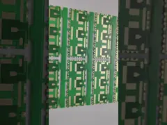
PCB information:
Material:AIN ceramic 1860
Layer:2
Surface finish:immersion gold
Thickness:1.0mm
Mark: Reflective Transparent Glass layer
To design a customized PCB, you'll need to follow these general steps:
Schematic Design: Create a schematic diagram of your circuit using a PCB design software. This step involves selecting and connecting the desired components, such as microcontrollers, sensors, ICs, resistors, capacitors, etc. If you already have a schematic, you can skip this step.
PCB Layout Design: Once the schematic is complete, you'll need to create the physical layout of the PCB. This involves placing the components on the board and routing traces to connect them according to the schematic. Consider factors like component placement for optimal signal flow, power and ground planes, and any mechanical constraints.
Component Placement: Carefully place the components on the PCB layout, taking into account factors such as signal integrity, thermal management, and space constraints. Ensure proper clearances between components and adherence to design guidelines for each component.
Routing: Establish connections between components by routing traces on the PCB. Pay attention to signal integrity, impedance control, and avoiding signal crosstalk. Use appropriate trace widths, vias, and layer stack-up to meet your design requirements.
Design Rule Check (DRC): Run a design rule check to ensure your PCB layout complies with the fabrication and assembly constraints. This step helps identify errors or violations like clearance violations, unconnected nets, or overlapping components.
Gerber File Generation: Generate the necessary Gerber files from your PCB design software. These files contain the manufacturing information for the PCB, including copper layers, solder mask, silkscreen, drill files, and more.
PCB Fabrication: Send the Gerber files to a PCB manufacturer or fabricator to produce the physical PCB. Choose a manufacturer that suits your requirements in terms of quality, cost, and turnaround time. Provide them with any additional specifications such as material type, board thickness, surface finish, and quantity.
PCB Assembly: Once you receive the fabricated PCBs, you can proceed with the assembly stage. This involves soldering the components onto the PCB. You can either do it yourself if you have the necessary skills and equipment or outsource it to a PCB assembly service.
It's important to note that designing a customized PCB requires knowledge of electronics, PCB design principles, and proficiency in PCB design software. If you are new to PCB design, it may be helpful to consult with an experienced engineer or work with a professional PCB design service.
If you have any specific requirements or questions during the design process, feel free to ask for assistance.