Company Profile
Infinites™ Tech Co.,Limited.is a research and
development,production,sales as one of the semiconductor storage
product solutions and Peripheral supporting productsprovider like PCB &PCBA,Prototype,TFT LCD integrated mill and Product assembling,but also the domestic few
can cover the DRAM and NAND Flash two major fieldsof high-tech enterprises,specialized new
enterprises.
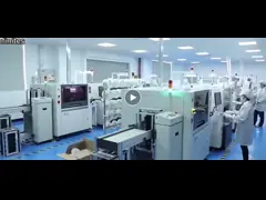
The company owns Infinites intelligent manufacturing production
base and Kingpins™ supply chain platform.Among them,Infinites™
intelligent manufacturing production base covers advanced chip
sealing and testing production line,module manufacturing production
line,technology research and development center and engineering
test center,which can provide one-stop service for product
packaging,testing,research and development design and production.
Infinites™ Tech as an excellent memory sealing test manufacturing
integration enterprise,proficient in BGA,LGA,SiP and other advanced packaging technology,and master a number of
packaging design simulation technology,self-developed test software
development,test algorithm,with a number of high quality module
manufacturing production line,With a number of advanced packaging
technologies,high-end module manufacturing capabilities and
domestic leading wafer and chip testing capabilities,the company
mainly provides customers with
Consumer,Industrial,Enterprise,Automotive,Embedded and other
storage products,and has won wide recognition in the market.